Method for forming non-planar transistor

A transistor and non-planar technology, which is applied in the field of manufacturing non-planar transistor structures, can solve the problems of complex structure, high manufacturing difficulty, and difficulty, and achieve the effect of simple process

Active Publication Date: 2013-03-27
UNITED MICROELECTRONICS CORP
View PDF5 Cites 10 Cited by
  • Summary
  • Abstract
  • Description
  • Claims
  • Application Information

AI Technical Summary

Problems solved by technology

However, since the fin transistor is a three-dimensional structure, it is more complicated than the traditional structure, and the manufacturing difficulty is relatively high. Generally, it is usually formed on a silicon-on-insulator (SOI) substrate. If it is to be compatible with the existing silicon The base process has a certain degree of difficulty
Moreover, due to the special manufacturing method of fin transistors, certain problems will also be encountered when integrating with existing planar transistors.

Method used


Image

  • Method for forming non-planar transistor
  • Method for forming non-planar transistor
  • Method for forming non-planar transistor

Examples


Embodiment Construction

[0019] In order to enable those skilled in the art of the present invention to further understand the present invention, several preferred embodiments of the present invention are enumerated below, together with the accompanying drawings, to describe in detail the composition and desired effects of the present invention.

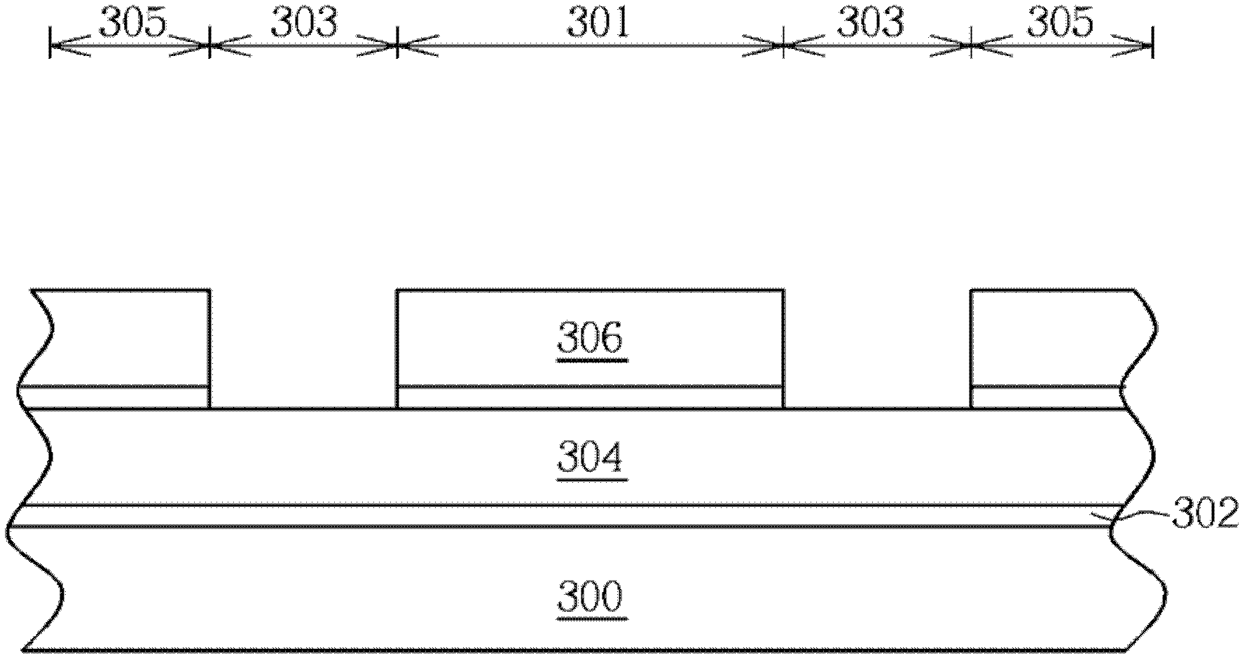
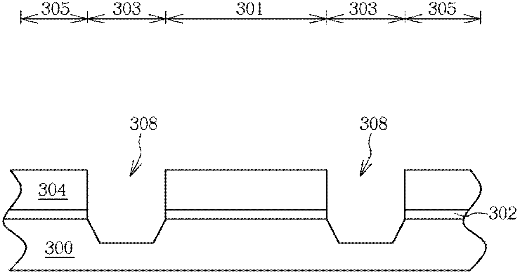
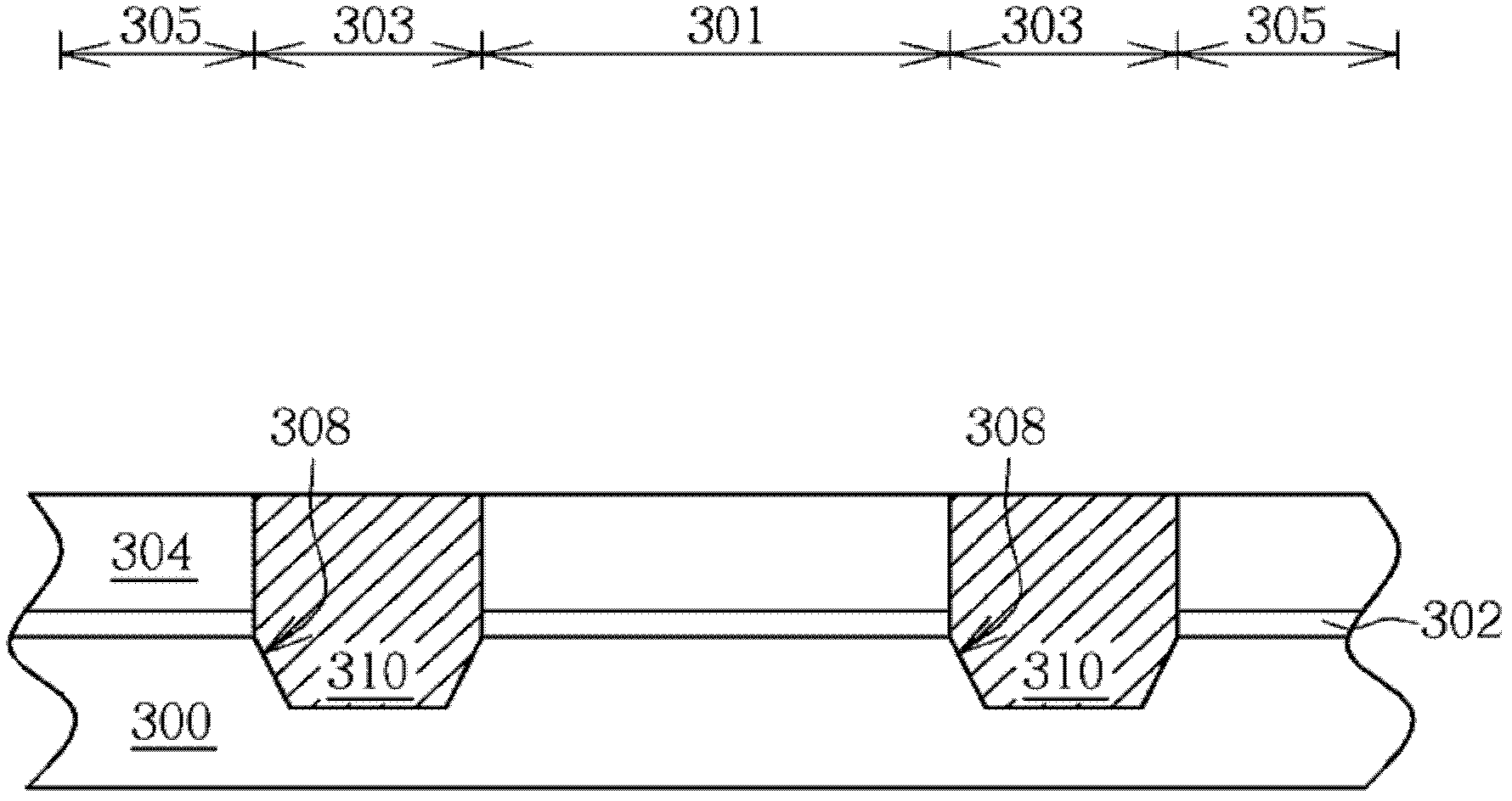
[0020] Please refer to Figure 1 to Figure 10 , is a schematic diagram of the steps of forming a non-planar transistor according to the present invention. Such as figure 1 As shown, firstly, a substrate 300 is provided, and the substrate 300 may be a silicon substrate, an epitaxial silicon substrate, a silicon germanium substrate, a silicon carbide substrate or a silicon-on-insulator (SOI) substrate. silicon-on-insulator, SOI) substrate, etc., but not limited to the above. An active region 301 , an isolation region 303 surrounding the active region 301 , and a peripheral region 305 are defined on the substrate 300 . The active region 301 is a region for p...


PUM


Abstract

The invention provides a method for forming a non-planar transistor. The method includes: firstly, providing a substrate defining an active region and a peripheral region, with a plurality of ultra-shallow channel isolators connected to the active region of the substrate; secondly, removing the ultra-shallow channel isolators to expose part of a sidewall of the substrate; forming a conductive layer on the active region and the peripheral region on the substrate to cover the part of the sidewall of the substrate; patterning the conductive layer to allow the conductive layer to form a gate of a planar transistor in the peripheral region and form a gate of at least one non-planar transistor in the active region; and forming a source and a drain on two sides of the gate of each non-planar transistor.

Description

technical field [0001] The invention relates to a method for making a non-planar transistor structure, in particular to a method capable of simultaneously forming a non-planar transistor and a planar transistor. Background technique [0002] In recent years, with the continuous miniaturization of various consumer electronic products, the design size of semiconductor components has also been continuously reduced to meet the trend and product requirements of high integration, high efficiency and low power consumption. [0003] However, with the miniaturization of electronic products, the existing planar transistors cannot meet the requirements of the products. Therefore, a non-planar fin transistor (Fin-FET) technology has been developed, which has a three-dimensional gate channel (channel) structure, which can effectively reduce the leakage of the substrate and reduce the short channel. effect, and has a higher drive current. However, since the fin transistor is a three-dim...

Claims


Application Information

Patent Timeline
Patent Type & Authority Applications(China)
IPC IPC(8): H01L21/336H01L21/28H01L21/762
Inventor 戴圣辉黄瑞民蔡振华蔡世鸿林建廷
Owner UNITED MICROELECTRONICS CORP
Why Eureka
Try Eureka