Non-planar semiconductor structure and process for same

A semiconductor and non-planar technology, which is applied in the direction of semiconductor devices, semiconductor/solid-state device manufacturing, electrical components, etc., can solve the problems of limited epitaxial layer total volume, metal silicide is not easy to adhere, and cannot be bonded, so as to increase the volume, Ease of adhesion, effect of increasing surface area

Active Publication Date: 2013-03-27
UNITED MICROELECTRONICS CORP
View PDF5 Cites 9 Cited by
  • Summary
  • Abstract
  • Description
  • Claims
  • Application Information

AI Technical Summary

Problems solved by technology

However, due to the difference in material between the epitaxial layer and the insulating structure, the two will repel each other and cause the epitaxial layer to have a take-off angle of nearly 54.8° of the crystal plane, so that the two cannot be bonded; in other words, because the epitaxial layer will be relatively insulating. Grows upwards at an oblique angle, thus limiting the total volume grown by the epitaxial layer
Furthermore, this structure also makes it difficult for subsequent metal silicides to adhere to it.

Method used


Image

  • Non-planar semiconductor structure and process for same
  • Non-planar semiconductor structure and process for same
  • Non-planar semiconductor structure and process for same

Examples


Embodiment Construction

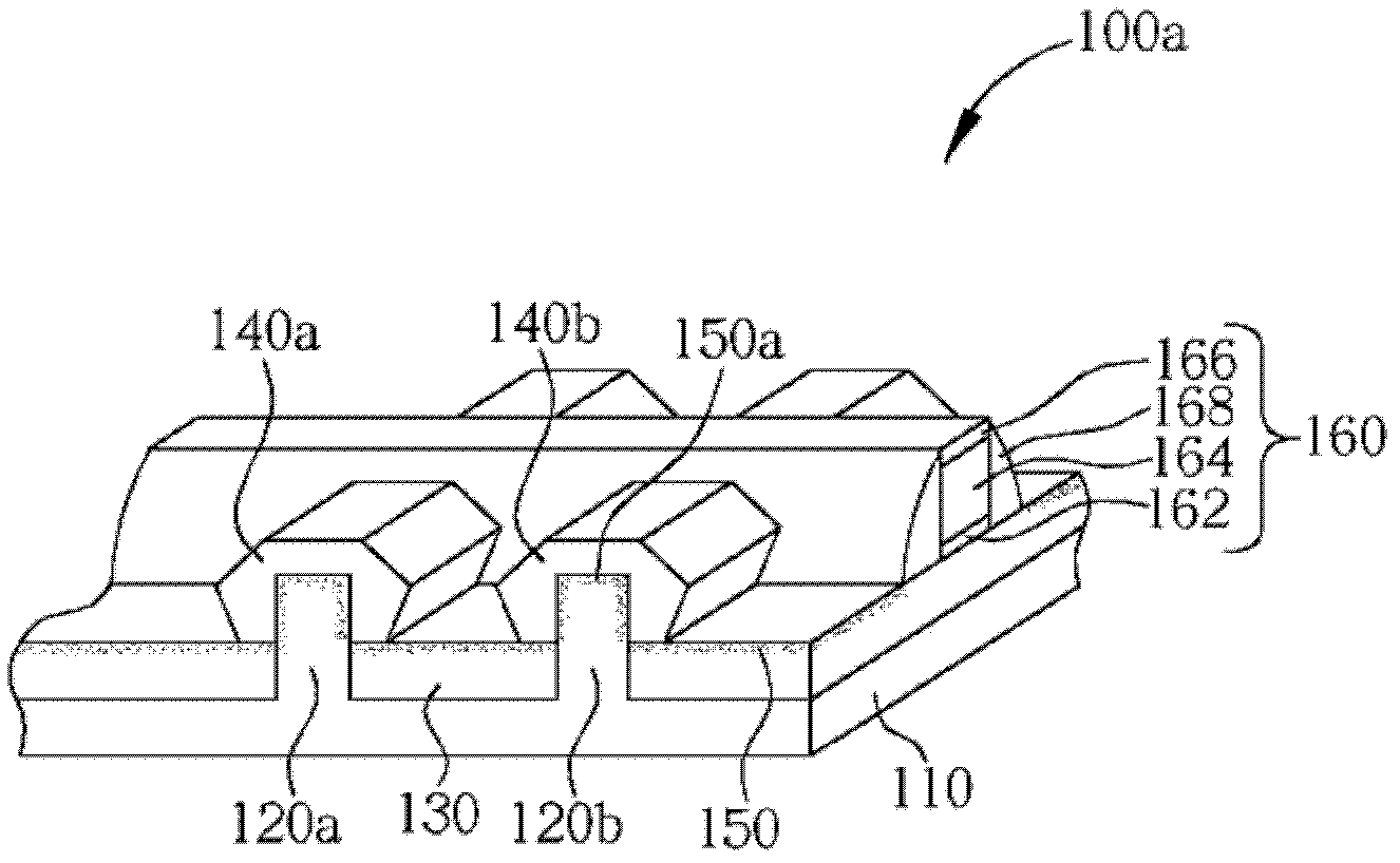
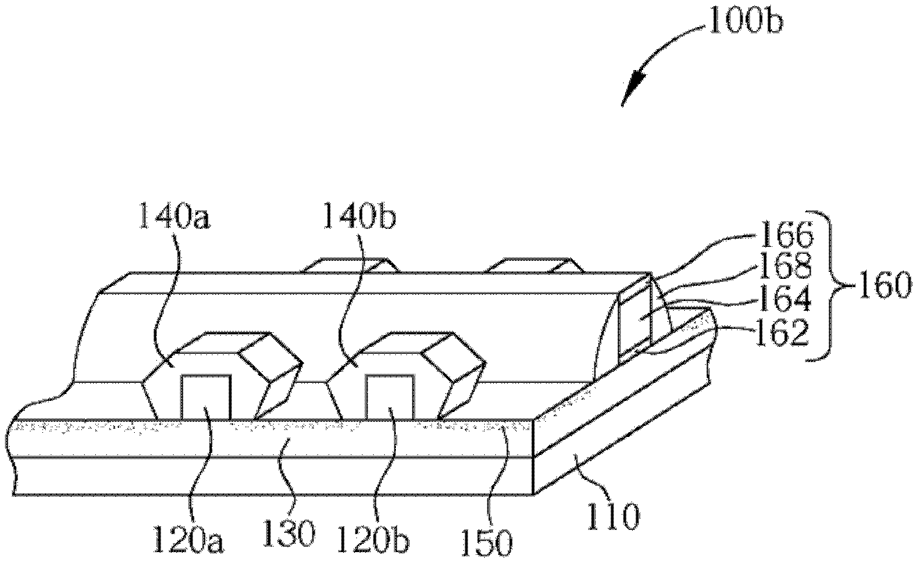
[0024] figure 1 A schematic cross-sectional view of a semiconductor structure containing a silicon substrate according to an embodiment of the present invention is shown. figure 2 A schematic cross-sectional view of a semiconductor structure including a silicon-on-insulator substrate according to another embodiment of the present invention is shown. see Figure 1-2 Both the semiconductor structures 100a and 100b include a substrate 110, two fin structures 120a and 120b, an insulating structure 130, and two epitaxial layers 140a and 140b. The fin structures 120 a and 120 b are located on the substrate 110 . The insulating structure 130 is located between the fin structures 120a and 120b. The insulating structure 130 has a nitrogen-containing layer 150 . The epitaxial layers 140 a and 140 b respectively cover part of the fin structures 120 a and 120 b and are located on the nitrogen-containing layer 150 . Figure 1-2 Only two fin structures 120a and 120b are shown, but the...


PUM


Abstract

The invention discloses a non-planar semiconductor structure and a process for the same. The non-planar semiconductor structure comprises a substrate, at least two fin-shaped structures, at least one insulating structure and a plurality of epitaxial layers. The fin-shaped structures are positioned on the substrate. The insulating structures are positioned among the fin-shaped structures and are provided with nitrogenous layers. The epitaxial layers respectively cover parts of the fin-shaped structures and are positioned on the nitrogenous layers.

Description

technical field [0001] The invention relates to a semiconductor structure and its technology, in particular to a semiconductor structure and its technology in which a nitrogen-containing layer is formed on the contact surface of an insulating structure and an epitaxial layer. Background technique [0002] As the size of semiconductor devices shrinks, maintaining the performance of small-sized semiconductor devices is a major goal of the industry. In order to improve the performance of semiconductor devices, various Fin-shaped field effect transistors (FinFETs) have been gradually developed. FinFET devices include the following advantages. Firstly, the fin field effect transistor process can be integrated with the traditional logic element process, so it has considerable process compatibility; secondly, because the three-dimensional shape of the fin structure increases the contact area between the gate and the substrate, it can increase The gate controls the charge in the c...

Claims


Application Information

Patent Timeline
Patent Type & Authority Applications(China)
IPC IPC(8): H01L29/78H01L21/336
Inventor 蔡世鸿林建廷简金城林进富刘志建蔡腾群吴俊元
Owner UNITED MICROELECTRONICS CORP
Why Eureka
Try Eureka