Metal or semiconductor structure on flexible substrate and annealing method of metal or semiconductor

A flexible substrate and metal structure technology, applied in semiconductor/solid-state device manufacturing, electrical components, circuits, etc., can solve the problems of flexible substrate damage, long operation time, high energy consumption, etc., and achieve uniform heating and heating energy consumption. Efficient effect

Active Publication Date: 2013-04-03
FUDAN UNIV
View PDF6 Cites 9 Cited by
  • Summary
  • Abstract
  • Description
  • Claims
  • Application Information

AI Technical Summary

Problems solved by technology

[0003] However, since the flexible substrate also has the disadvantage of low temperature resistance, and the temperature used in the annealing process is still too high, the traditional annealing method may still cause damage to the flexible substrate, such as the generation of gas, water, etc. Vapor, etc., not suitable for the preparation of semiconductor structures on flexible substrates
Moreover, the traditional annealing method takes a long time to operate and consumes a lot of energy.

Method used


Image

  • Metal or semiconductor structure on flexible substrate and annealing method of metal or semiconductor
  • Metal or semiconductor structure on flexible substrate and annealing method of metal or semiconductor
  • Metal or semiconductor structure on flexible substrate and annealing method of metal or semiconductor

Examples


Embodiment Construction

[0021] In order to make the objectives, technical solutions, and advantages of the present invention clearer, the various embodiments of the present invention will be described in detail below with reference to the accompanying drawings. However, a person of ordinary skill in the art can understand that, in each embodiment of the present invention, many technical details are proposed for the reader to better understand the present application. However, even without these technical details and various changes and modifications based on the following embodiments, the technical solutions claimed by the claims of this application can be realized.

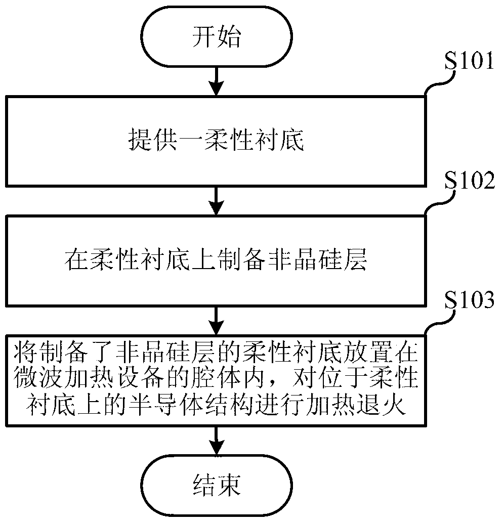
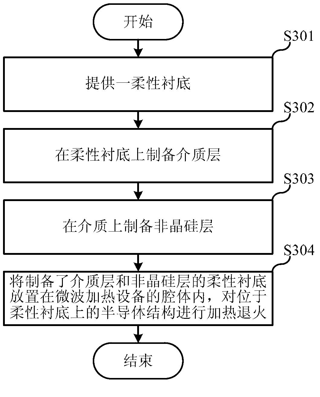
[0022] The first embodiment of the present invention relates to a method for annealing a semiconductor structure on a flexible substrate. The specific process is as follows figure 1 Shown.

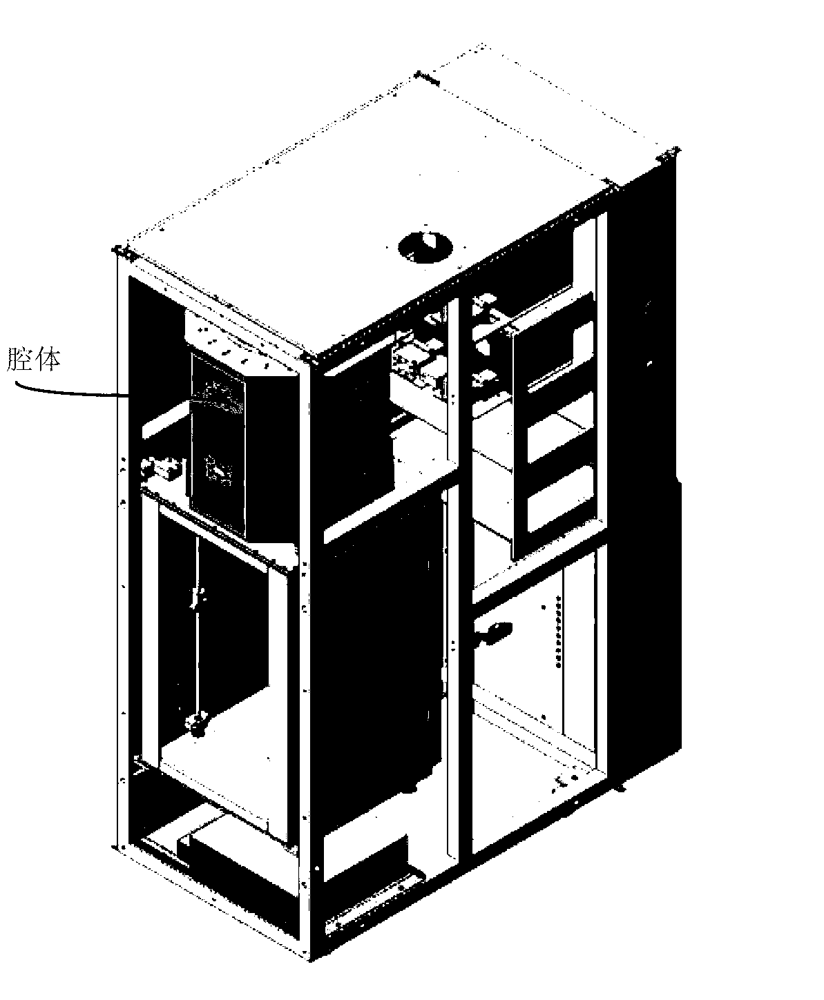
[0023] Step S101, providing a flexible substrate. Specifically, the flexible substrate may be formed of a material with a lower cost and a lower upper ...


PUM

PropertyMeasurementUnit
depthaaaaaaaaaa
depthaaaaaaaaaa

Abstract

The invention relates to the technical field of a semiconductor technology, and discloses a metal or semiconductor structure on a flexible substrate and an annealing method of the metal or semiconductor structure. According to the annealing method, the metal or semiconductor structure on the flexible substrate is annealed in a microwave heating manner; as microwave heating has the characteristic of selective heating on a material, when the metal or semiconductor structure on the flexible substrate is annealed, an amorphous silicon layer or a meta layer can be selectively heated, the flexible substrate does not absorb or basically does not absorb microwave energy, and therefore, the flexible substrate is not heated to a very high temperature during microwave annealing, thus the flexible substrate is prevented from being damaged; and the microwave heating can ensure that the interior and the exterior of the heated material are simultaneously heated, and the heating is uniform. Thus, according to the method, the metal or semiconductor structure on the flexible substrate can be annealed, the heating is uniform, and the efficiency of heating energy consumption is high.

Description

Technical field [0001] The present invention relates to the technical field of semiconductor technology, in particular to a metal or semiconductor structure on a flexible substrate and an annealing method thereof. Background technique [0002] Compared with amorphous silicon, the carrier mobility of polycrystalline silicon is increased by two orders of magnitude, so it is widely used in the production of thin film field effect transistors (Thin Film Transistor, referred to as "TFT"). The preparation method of polysilicon is usually as follows: first prepare an amorphous silicon layer on the substrate, and then anneal to obtain polysilicon. The preparation method of polysilicon can be divided into high temperature preparation and low temperature preparation according to the preparation temperature. Since the temperature during high-temperature annealing will exceed 1000 degrees, it is well known that at this high temperature, the glass substrate or the plastic substrate will soft...

Claims


Application Information

Patent Timeline
Patent Type & Authority Applications(China)
IPC IPC(8): H01L21/20H01L21/268
Inventor 吴东平许鹏付超超赵丹张卫张世理
Owner FUDAN UNIV
Why Eureka
Try Eureka