Method for detecting semiconductor device electrical property failure

A technology of electrical failure and detection method, which is applied in the direction of semiconductor/solid-state device testing/measurement, etc., can solve problems such as difficulty in finding online problems in time, problem lag, and electrical failure of semiconductor devices, and achieve the effect of shortening the research and development cycle

Active Publication Date: 2013-04-03
SHANGHAI HUALI MICROELECTRONICS CORP
View PDF4 Cites 20 Cited by
  • Summary
  • Abstract
  • Description
  • Claims
  • Application Information

AI Technical Summary

Problems solved by technology

[0005] The present invention aims at providing a detection method for the electrical failure of a semiconductor device in the prior art, where the traditional semiconductor device electrical testing method lags behind in finding problems, and it is difficult to find defects such as online problems in time

Method used


Image

  • Method for detecting semiconductor device electrical property failure
  • Method for detecting semiconductor device electrical property failure
  • Method for detecting semiconductor device electrical property failure

Examples


Embodiment Construction

[0023] In order to illustrate the technical content, structural features, achieved goals and effects of the present invention in detail, the following will be described in detail in conjunction with the embodiments and accompanying drawings.

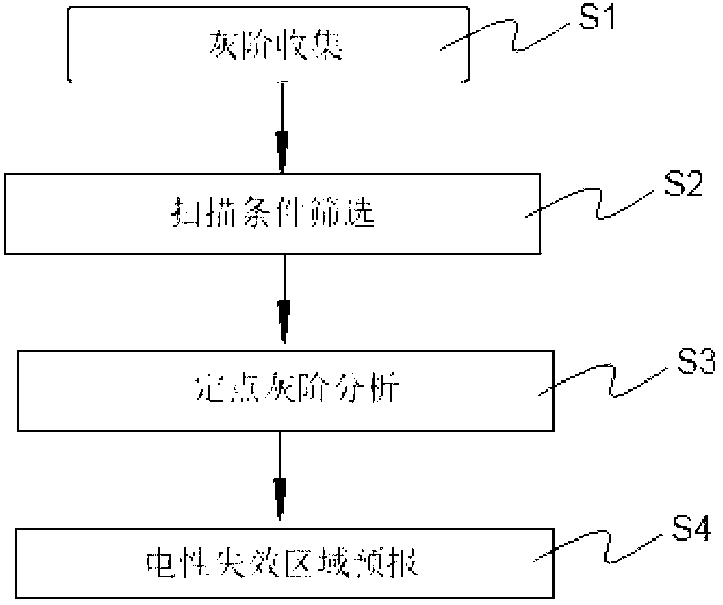
[0024] see figure 1 , figure 1 Shown is a flow chart of the detection method for the electrical failure of the semiconductor device of the present invention. The detection method for the electrical failure of the semiconductor device comprises the following steps:

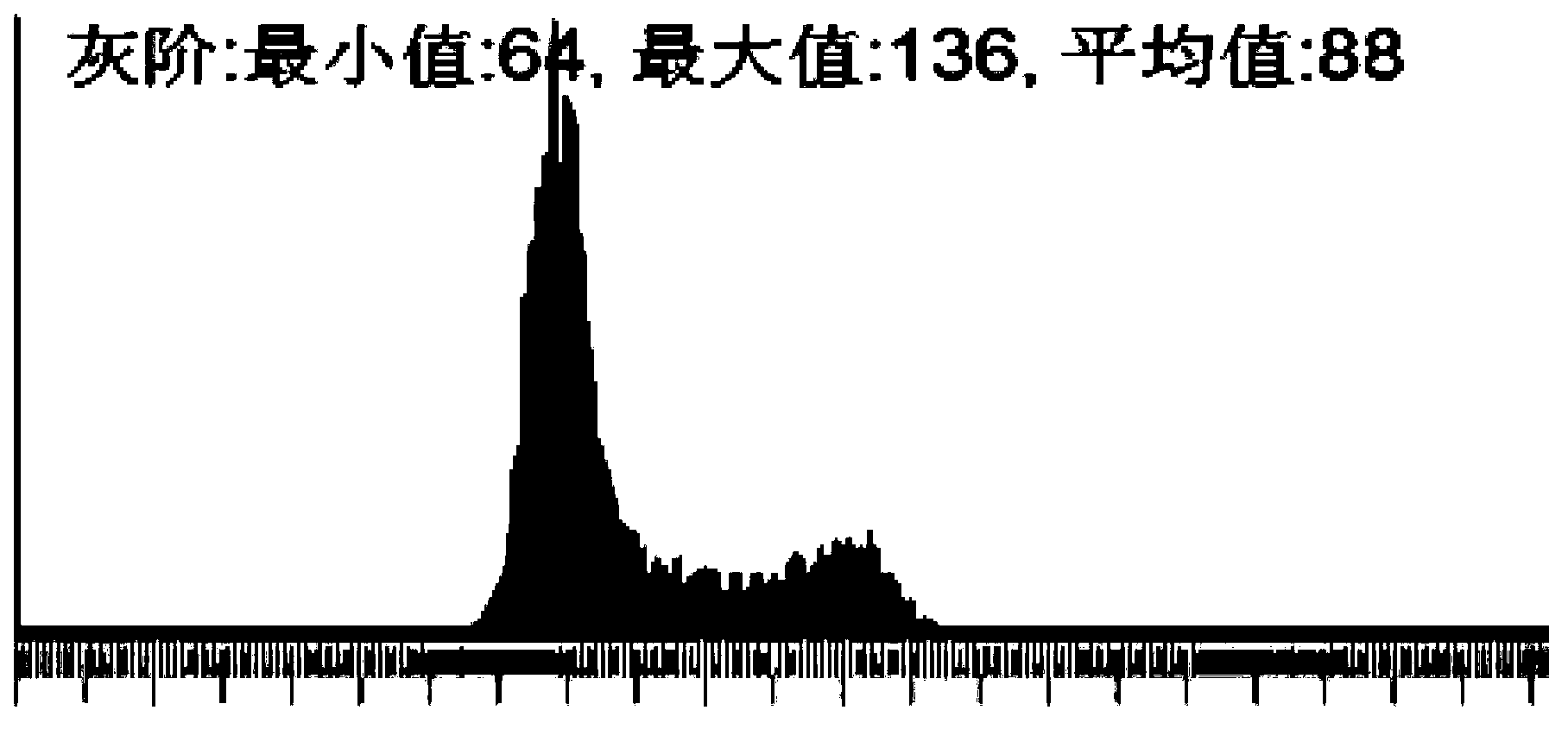
[0025] Executing step S1: grayscale collection; specifically, the grayscale collection further includes: a. Applying an electron beam defect scanner to establish a fixed-point scanning program on the metal connection layer of the semiconductor device, and selecting the internal area of ​​the repeating unit in the module to be tested , taking the smallest area that can be scanned by the electron beam defect scanner as the scanning unit area, the scanning unit area is detecte...


PUM


Abstract

The invention discloses a method for detecting a semiconductor device electrical property failure. The method for detecting the semiconductor device electrical property failure comprises the following steps of: S1, collecting the gray scale: a. taking the minimum region which can be scanned by an electron beam defect scanner as a scanning unit region, setting as a defect through a program form and detecting the defect, and shooting an electron microscope atlas; and b. taking a semiconductor device as a scanning object, scanning under different conditions, and analyzing the gray scale; S2, screening scanning conditions, and testing the electrical property of the scanning conditions; acquiring a similarity numerical value; and defining the optimal scanning condition; S3, carrying out fixed point gray scale analysis so as to obtain a gray scale data collecting interval with an effective electrical property; and S4, forecasting an electrical property failure region. According to the invention, the gray scale collected data obtained by the electron beam defect scanner and the electrical property testing data are compared, the electrical property failure region and an electrical property effective region can be forecast effectively, which provides a basis for monitoring the advantages and disadvantages of an ion implantation technology, provides a technical support for to-be-adopted improving measures, and provides a powerful guarantee for shortening the research cycle of the semiconductor device.

Description

technical field [0001] The invention relates to the technical field of semiconductor devices, in particular to a method for detecting electrical failure of semiconductor devices. Background technique [0002] The ion implanter is one of the most critical doping equipment in the manufacture of semiconductor devices. It is a device that guides impurities into the semiconductor wafer to change the conductivity of the wafer. Among them, the uniformity of depth and density of impurity implantation directly determines the quality of the implanted wafer. The uniformity control technology of the ion implanter is one of the key technologies of the ion implanter. Its working principle is to uniformly and accurately implant ions into the entire wafer surface according to the set dose based on various control and measurement methods and devices. [0003] The quality of ion implantation of semiconductor devices plays a key role in the quality of semiconductor devices. With the developme...

Claims


Application Information

Patent Timeline
Patent Type & Authority Applications(China)
IPC IPC(8): H01L21/66
Inventor 范荣伟顾晓芳倪棋梁龙吟陈宏璘
Owner SHANGHAI HUALI MICROELECTRONICS CORP
Why Eureka
Try Eureka