Supercharge Your Innovation With Domain-Expert AI Agents!

Semiconductor device and method for manufacturing semiconductor device

A semiconductor and device technology, applied in the field of manufacturing semiconductor devices, can solve problems such as radiation efficiency decline and absorption loss

Active Publication Date: 2016-11-02
OSRAM OPTO SEMICON GMBH & CO OHG
View PDF8 Cites 0 Cited by
  • Summary
  • Abstract
  • Description
  • Claims
  • Application Information

AI Technical Summary

Problems solved by technology

[0004] In radiation-emitting semiconductor components, for example in components with light-emitting diode chips for generating radiation, parts of the radiation scattered back, for example on lamp housings, can be absorbed in the component, as a result of which the overall efficiency of radiation generation is reduced
[0005] Especially in devices where the semiconductor chip is mounted directly on a flat carrier, significant losses can result due to carrier absorption

Method used


Image

  • Semiconductor device and method for manufacturing semiconductor device
  • Semiconductor device and method for manufacturing semiconductor device
  • Semiconductor device and method for manufacturing semiconductor device

Examples


Embodiment Construction

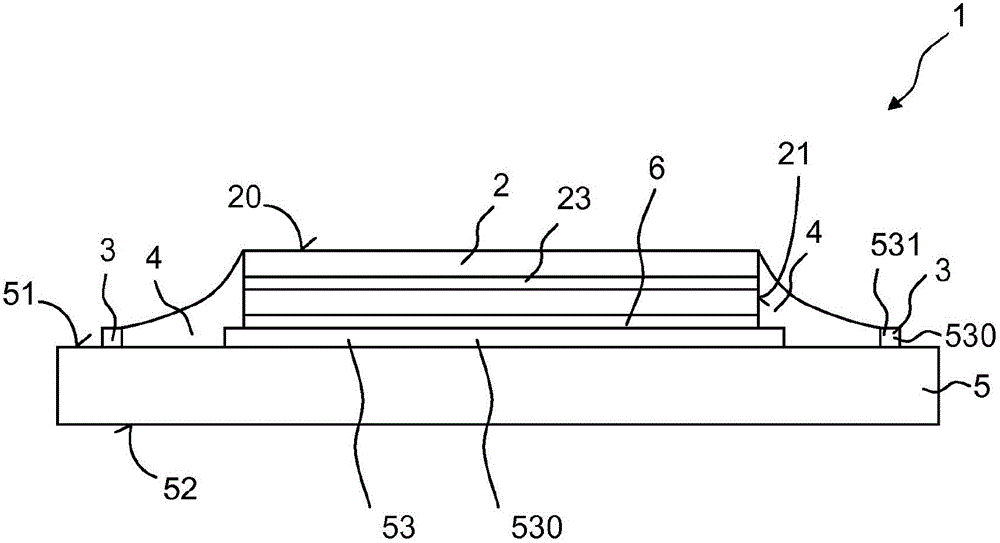
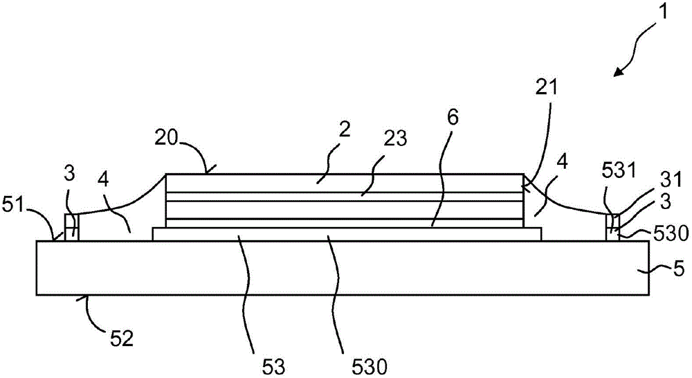
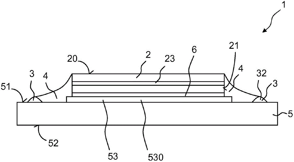
[0041] Elements that are identical, of the same type or perform the same function are provided with the same reference symbols in the figures.

[0042] The figures and the size ratios of the elements shown in the figures to one another are not to be regarded as being to scale. Conversely, individual elements, in particular layer thicknesses, can be shown exaggerated for better visibility and / or for better understanding.

[0043] exist figure 1 A first exemplary embodiment of a semiconductor component is schematically shown in cross-section in FIG. The semiconductor component 1 has a semiconductor chip 2 which is arranged on a connection surface 53 of a connection carrier 5 . The semiconductor chip is attached to the connection surface by means of the connection layer 6 . Thus, the semiconductor chips are fastened in a flat arrangement on the flat connection carrier without encapsulation.

[0044] The semiconductor chip 2 is designed as a light-emitting diode semiconductor...


PUM


Abstract

A semiconductor component (1) is proposed which has at least one optoelectronic semiconductor chip (2) and a connection carrier (5) with a connection area (53) on which the semiconductor chip (2) is arranged. A reflective layer (4) and a delimiting structure (3) are formed on the connection carrier (5), wherein the delimiting structure (3) surrounds the semiconductor chip (2) at least partially in lateral direction, and the reflective layer (4) In the lateral direction, it extends at least partially between the side surfaces ( 21 ) of the semiconductor chip and the delimiting structure ( 3 ). Furthermore, a method for manufacturing a semiconductor device is proposed.

Description

technical field [0001] The present application relates to a semiconductor device and a method for manufacturing the semiconductor device. [0002] Cross-References to Related Applications [0003] This application claims priority from German patent application 10 2010 031 945.7, the disclosure of which is hereby incorporated by reference. Background technique [0004] In radiation-emitting semiconductor components, for example in components with light-emitting diode chips for generating radiation, parts of the radiation scattered back, for example on lamp housings, can be absorbed in the component, as a result of which the overall efficiency of radiation generation is reduced . [0005] Particularly in components in which the semiconductor chip is mounted directly on a flat carrier, considerable losses can result due to absorption by the carrier. Contents of the invention [0006] The object is to propose a semiconductor device in which absorption losses are reduced. F...

Claims


Application Information

Patent Timeline
Patent Type & Authority Patents(China)
IPC IPC(8): H01L33/46H01L33/60
CPCH01L31/0232H01L31/18H01L33/46H01L33/60H01L2933/0025H01L33/44H01L33/58
Inventor 西蒙·耶雷比奇埃里克·海涅曼克里斯蒂安·盖特纳阿莱斯·马尔基坦
Owner OSRAM OPTO SEMICON GMBH & CO OHG
Features
  • R&D
  • Intellectual Property
  • Life Sciences
  • Materials
  • Tech Scout
  • Unparalleled Data Quality
  • Higher Quality Content
  • 60% Fewer Hallucinations
Learn More