Data communication method between processors and FPGA (field programmable gate array) equipment
A data communication and processor technology, applied in the field of data communication, can solve the problems of low real-time data exchange, slow access speed, complex dual-port RAM control logic, etc., and achieve the effect of flexible logic implementation and high cost performance.
- Summary
- Abstract
- Description
- Claims
- Application Information
AI Technical Summary
Problems solved by technology
Method used
Image
Examples
Embodiment 1
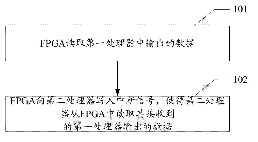
[0022] see figure 1 , figure 1 It is a flow chart of the method in Embodiment 1 of the present invention. Such as figure 1 As shown, a data communication method between processors may include the following steps:
[0023] 101. The FPGA reads data output from the first processor.
[0024] Wherein, the FPGA is provided with a shared data block, and in one embodiment, the shared data block can be a block random access memory BlockRam, and adopts the basic principle of a standard dual-port RAM with an intellectual property module (IP, Intellectual Propertycore) core to realize the shared data block logical function. The shared data block has write competition logic, which can effectively avoid being written by mistake.
[0025] The clock of the shared data block can be input by an external 16MHz oscillator through a digital clock management unit (DCM, Digital Clock Manager) after phase-locking and frequency conversion.
[0026] Further, the data output by the first processor...
Embodiment 2
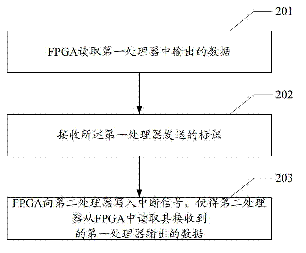
[0033] see figure 2 , figure 2 It is a flowchart of the method of Embodiment 2 provided by the present invention. Such as figure 2 As shown, a data communication method between processors, including:
[0034] 201. The FPGA reads data output from the first processor.
[0035] Wherein, the internal structure principles and logic functions of the FPGA can refer to the description in Step 101 of Embodiment 1, and the embodiments of the present invention will not be repeated here.
[0036] 202. Receive an identifier sent by the first processor.
[0037] Wherein, the identifier is sent by the first processor after the FPGA finishes reading the data output by the first processor. The identification is used to trigger the step of FPGA writing an interrupt signal to the second processor (that is, step 203 in this embodiment).
[0038] In an embodiment, the identifier sent by the first processor may be read by the shared data block of the FPGA, and the identifier may be 0x55AA....
PUM
 Abstract
Description
Claims
Application Information


