
Semiconductor light-emitting device and manufacturing method of the same

A technology of light-emitting devices and semiconductors, which is applied to semiconductor devices, electric solid-state devices, electrical components, etc., and can solve the problems of reduced output, picking failure, and the inability of robotic equipment to pick up semiconductor light-emitting devices.

Inactive Publication Date: 2013-04-10
KK TOSHIBA
View PDF5 Cites 2 Cited by
  • Summary
  • Abstract
  • Description
  • Claims
  • Application Information

AI Technical Summary

Problems solved by technology

However, at this stage, since the surface of the wavelength conversion unit is roughened by etching, air may enter the surface undesirably through gaps in the irregular surface.
When this happens, robotic equipment will not be able to pick and / or reliably deliver semiconductor light emitting devices
Resulting pick failures lead to lower yields

Method used


Image

  • Semiconductor light-emitting device and manufacturing method of the same
  • Semiconductor light-emitting device and manufacturing method of the same
  • Semiconductor light-emitting device and manufacturing method of the same

Examples


Embodiment Construction

[0017] Here, a semiconductor light emitting device having a plurality of light emitting units (ie, a multi-chip type semiconductor light emitting device) is exemplified.

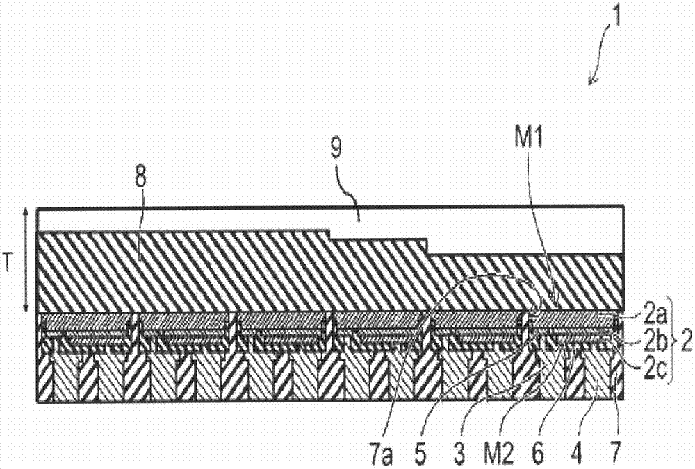
[0018] figure 1 is a cross-sectional view illustrating a semiconductor light emitting device 1 manufactured according to an embodiment disclosed herein. Such as figure 1 As shown, in a semiconductor light emitting device 1 , a light emitting unit 2 , an electrode part 3 , an electrode part 4 , a bonding part 5 , a lead part 6 , a sealing part 7 and a wavelength conversion unit 8 are provided. The light emitting unit 2 comprises a plurality of light emitting subunits which, when used together, constitute the light emitting unit 2 . Although the semiconductor light emitting device 1 may include a plurality of light emitting units 2, only a single light emitting unit 2 is described in detail herein.

[0019] The light emitting unit 2 includes a main surface M1 and a main surface M2. The main surface M2 is o...


PUM


Abstract

According to one embodiment, a light-emitting unit (2) which emits light, a wavelength conversion unit (8) which includes a phosphor and which is provided on a main surface of the light-emitting unit, and a transparent resin (9) which is provided on top of the wavelength conversion unit, are prepared. The transparent resin has a greater modulus of elasticity and / or a higher Shore hardness than the wavelength conversion unit (8).

Description

[0001] Cross References to Related Applications [0002] This application is based on and claims priority from Japanese Patent Application No. 2012-078364 filed on 03 / 29 / 12; the entire contents of which are hereby incorporated by reference. technical field [0003] Embodiments described herein relate to semiconductor light emitting devices and methods of manufacturing the same. Background technique [0004] In one example, a semiconductor light-emitting device has a semiconductor element (hereinafter simply referred to as a light-emitting element), a wavelength conversion unit including a phosphor, a light-emitting element that emits blue light such as a blue LED (light-emitting diode), and, for example, emits light complementary to blue light. Phosphor of yellow light. Use these parts together for white light. Other phosphors emitting light of other wavelengths (ie colors) can also be combined into the wavelength conversion unit in this way to obtain other colors by combi...

Claims


Application Information

Patent Timeline
IPC IPC(8): H01L33/56
CPCH01L27/15H01L2933/0041H01L33/505H01L33/54H01L33/508H01L33/502H01L33/56
Inventor 中山俊弥樋口和人小泉洋西内秀夫小幡进木村晃也杉崎吉昭小岛章弘秋元阳介
Owner KK TOSHIBA
Learn More