Soldering Offset Prevention Method for Surface Mount Devices

A technology of surface mount devices and surface mount devices, which is applied in the field of anti-soldering offset of surface mount devices, can solve problems such as easy generation of tin balls, easy displacement, and chip offset, so as to avoid repair work and avoid device Offset, the effect of improving work efficiency

Active Publication Date: 2015-08-12
JIANGNAN INST OF COMPUTING TECH
View PDF3 Cites 0 Cited by
  • Summary
  • Abstract
  • Description
  • Claims
  • Application Information

AI Technical Summary

Problems solved by technology

[0005] TO265 packaged devices often generate a lot of heat when they work, so the grounding pad designed on the PCB board (Printed Circuit Board, also known as printed circuit board, printed circuit board) is often 1-2 times larger than the actual device , this solder pad is prone to produce tin beads during soldering, and the tension is high during reflow, which is easy to cause displacement; that is, although the conventional stencil opening design meets the requirements for the amount of solder paste, there is a phenomenon of chip offset after reflow soldering
The common pad opening is 1:1 opening, but the results after soldering show that deviation is very easy to occur
This undoubtedly brings unnecessary efficiency loss to production. In order to ensure reliability and reduce defect rate at the same time, it is an inevitable choice to find a more suitable opening method.

Method used


Image

  • Soldering Offset Prevention Method for Surface Mount Devices
  • Soldering Offset Prevention Method for Surface Mount Devices
  • Soldering Offset Prevention Method for Surface Mount Devices

Examples


Embodiment Construction

[0025] In order to make the content of the present invention clearer and easier to understand, the content of the present invention will be described in detail below in conjunction with specific embodiments and accompanying drawings.

[0026] The inventors of the present invention have advantageously found that in the existing surface mount process, the reason why surface mount devices such as TO265 packaged devices are prone to offset is mainly due to the fact that the center of the solder paste printing is aligned with the surface mount device. The actual placement center does not coincide.

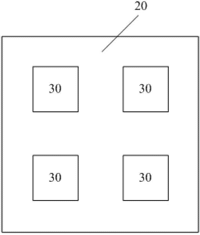
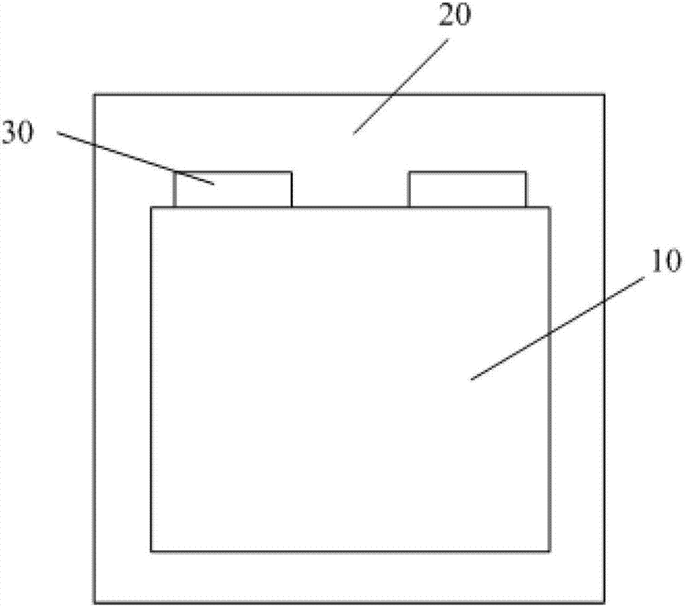
[0027] Specifically, the design of existing surface mount devices such as TO265 package devices and the like is that, at the central position of the pad 20 of the PCB board, a grid-shaped opening 30 is opened, and solder paste is printed on the PCB, such as figure 2 shown.

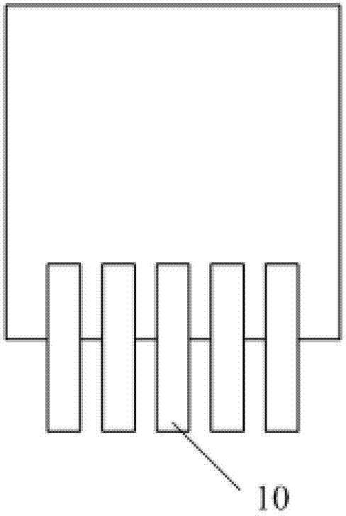
[0028] However, since the grounding pads of surface mount devices such as TO265 packaged devices are generally ...


PUM


Abstract

A welding skewing-proof method for a surface mounting device comprises the following steps: (1) making a steel mesh and utilizing surface mount technology (SMT) printing equipment to cover welding paste on a printed circuit board (PCB) surface, thereby enabling a steel mesh opening which is served as the center of the welding paste printing to overlap the actual center point of surface installation device paster, (2) pasting the paster, using the SMT paster equipment to place the to-be-installed surface mounting device on a corresponding position of a PCB plate so as to enable a leading foot of the to-be-welded surface mounting device to cover the whole welding paste, (3) conducting reflow soldering, utilizing reflow furnace equipment, and by means of concrete curve heating arrangement, enabling the welding paste to be converted and form eutectic soldered dots.

Description

technical field [0001] The invention relates to the field of semiconductor packaging, and more specifically, the invention relates to a method for preventing solder offset of surface mount devices. Background technique [0002] Surface Mounted Technology (SMT) is currently the most popular technology and process in the electronics assembly industry. [0003] In the surface mount process, solder paste printing is the first link in the entire process, and the printing quality will directly affect the pass-through rate of surface mount products. According to statistics, 60%-70% of welding defects are directly related to the printing quality, and among the various factors affecting the printing process, the design and production technology of the printing stencil plays a pivotal role. [0004] There are TO265 packaged devices in SMT welding, and its appearance is as follows figure 1 As shown, the number 10 represents the part of the surface mount device pin (pin) to be soldere...

Claims


Application Information

Patent Timeline
Patent Type & Authority Patents(China)
IPC IPC(8): H05K3/34
Inventor 王彦桥吴小龙孙忠新高锋刘晓阳张涛梁少文
Owner JIANGNAN INST OF COMPUTING TECH
Why Eureka
Try Eureka