Encapsulating substrate structure provided with coupling circuit

A technology for packaging substrates and coupling lines, which is applied in the direction of circuits, printed circuit components, electrical components, etc.

Inactive Publication Date: 2013-04-17
ADVANCED SEMICON ENG INC
View PDF3 Cites 2 Cited by
  • Summary
  • Abstract
  • Description
  • Claims
  • Application Information

AI Technical Summary

Problems solved by technology

[0005] In view of this, the present invention provides a package substrate structure with coupling lines to solve the problem of impedance matching in the prior art

Method used


Image

  • Encapsulating substrate structure provided with coupling circuit
  • Encapsulating substrate structure provided with coupling circuit
  • Encapsulating substrate structure provided with coupling circuit

Examples


Embodiment Construction

[0015] The following descriptions of the various embodiments refer to the accompanying drawings to illustrate specific embodiments in which the present invention can be practiced. Furthermore, the directional terms mentioned in the present invention are, for example, up, down, top, bottom, front, back, left, right, inside, outside, side, surrounding, central, horizontal, transverse, vertical, longitudinal, axial, The radial direction, the uppermost layer or the lowermost layer, etc. are only directions referring to the attached drawings. Therefore, the directional terms used are used to illustrate and understand the present invention, but not to limit the present invention.

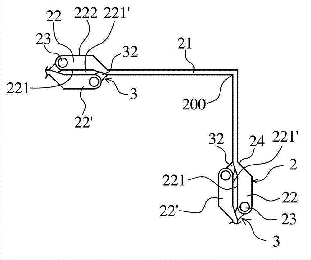
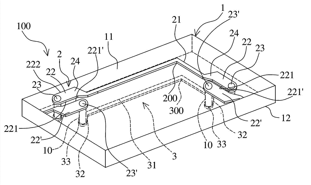
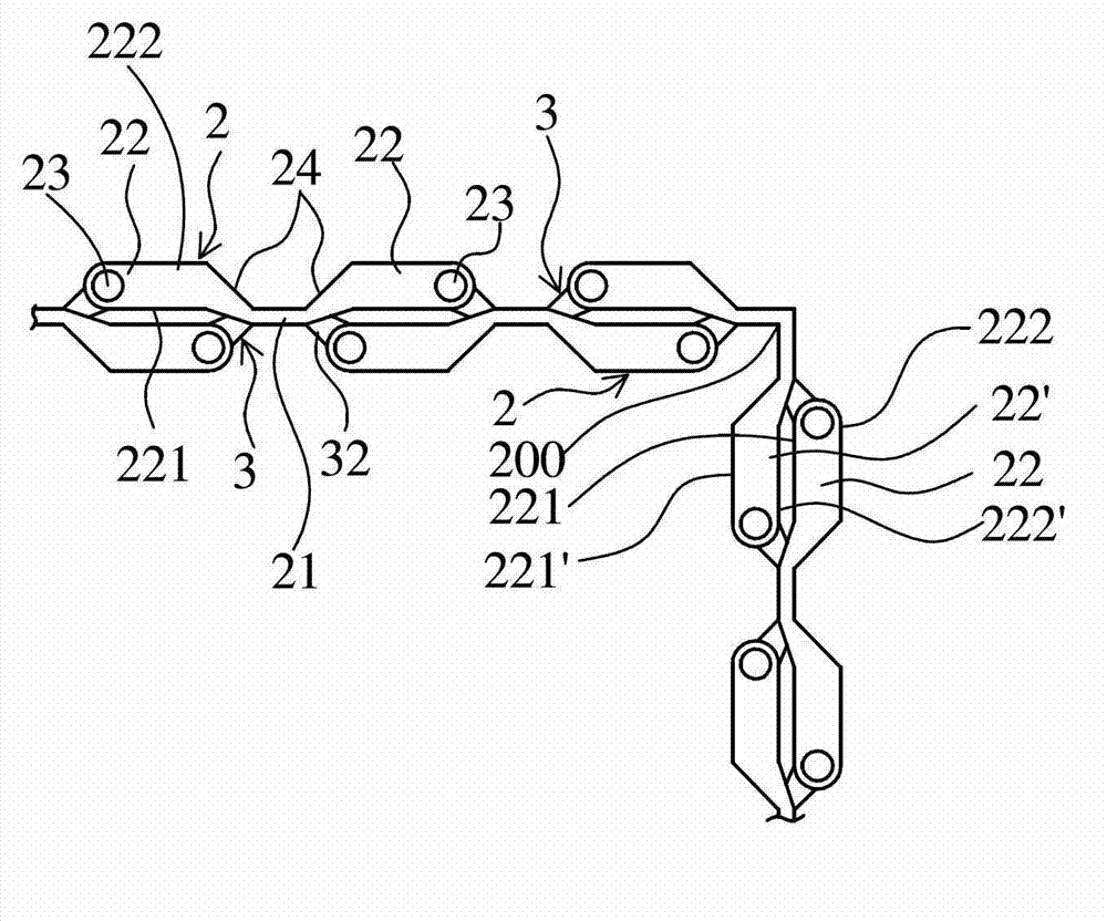
[0016] Please refer to figure 1 and 2 As shown, the packaging substrate structure 100 with coupling lines according to an embodiment of the present invention mainly includes a dielectric layer 1, a plurality of upper layer circuit units 2, a plurality of lower layer circuit units 3 and a plurality of co...


PUM


Abstract

The invention discloses an encapsulating substrate structure provided with a coupling circuit. The encapsulating substrate structure comprises a dielectric layer, a plurality of upper layer circuit units, a plurality of lower layer circuit units and a plurality of current conducting holes, wherein the upper layer circuit units are arranged on the upper surface of the dielectric layer, and are arranged in sequence at certain intervals; the same-layer coupling segment of each upper layer circuit unit and the same-layer coupling segment of another upper layer circuit unit are adjacent to each other, and are arranged in parallel with one another; the lower layer circuit units are arranged on the lower surface of the dielectric layer, and are arranged in sequence at certain intervals; and a hybrid differential motion design is realized by coupling two differential circuits on the same layer and coupling two differential circuits in adjacent layers without adjusting impedance matching, so that a high electric characteristic can be kept.

Description

technical field [0001] The present invention relates to a package substrate structure, in particular to a package substrate structure with coupling lines. Background technique [0002] On the printed circuit board and the packaging substrate, the signal line is electrically connected between two interfaces, two components or two terminals, and the line width must be consistent so that when the signal is transmitted between the lines, the characteristic impedance (characteristic impedance) can be maintained. Unchanged, especially in high-speed and high-frequency signal transmission, the reflection caused by good impedance matching between the two terminals is required to reduce the insertion loss of signal transmission and relatively improve the return of signal transmission. Loss (return loss), so as not to affect the quality of signal transmission. [0003] A general signal transmission structure includes a reference plane and two wires, the wires are spaced apart and have...

Claims


Application Information

Patent Timeline
Patent Type & Authority Applications(China)
IPC IPC(8): H01L23/498H05K1/02
Inventor 王陈肇
Owner ADVANCED SEMICON ENG INC
Why Eureka
Try Eureka