Method and structure for realizing balanced parallel connection of electronic switching devices

A technology for electronic switches and devices, applied in the field of realizing balanced parallel connection of electronic switching devices, can solve problems such as stability, reliability impact, parallel expansion limitation, large thermal stress difference, etc., to achieve balanced current, reduce the number of devices, and reduce electromagnetic interference. Effect

Active Publication Date: 2013-04-17
GUANGZHOU QINGTIAN INDAL
View PDF2 Cites 0 Cited by
  • Summary
  • Abstract
  • Description
  • Claims
  • Application Information

AI Technical Summary

Problems solved by technology

When connecting in parallel, it is very important to make each device flow an equal current. Once the current balance is destroyed, the device with too concentrated current may be damaged, which has a great impact on the stability and reliability of the power supply system. influences
However, in the current structure of parallel power electronic switching devices, the conductive paths are relatively long, and each path is isolated from each other, the length is different, the impedance is large, the loss is large, the current flowing through the components is different, and the thermal stress is greatly different. damage, then the device with too much current concentration will shorten its lifespan or even be damaged
[0004] At the same time, when the fast switching device is turned off, due to the inductance generated by its connecting conductor, a turn-off overvoltage will be generated on the switching device. Once the overvoltage is higher than the rated withstand voltage of the device, the device will be damaged, that is to say , in practice, the parallel expansion of switching devices is limited by the inductance of the connecting conductors

Method used


Image

  • Method and structure for realizing balanced parallel connection of electronic switching devices
  • Method and structure for realizing balanced parallel connection of electronic switching devices
  • Method and structure for realizing balanced parallel connection of electronic switching devices

Examples


Embodiment Construction

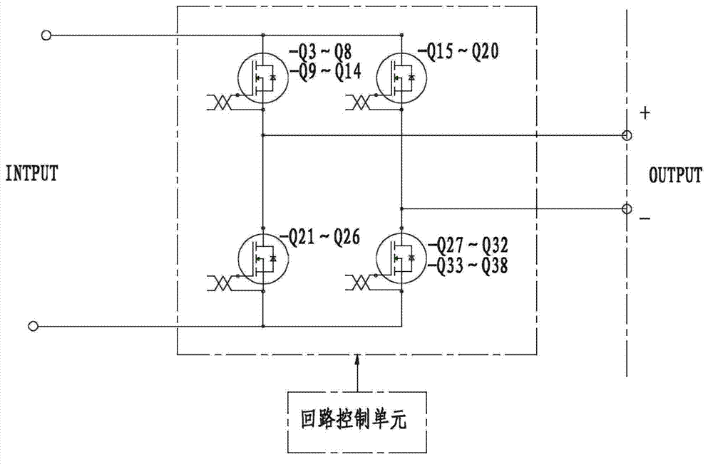
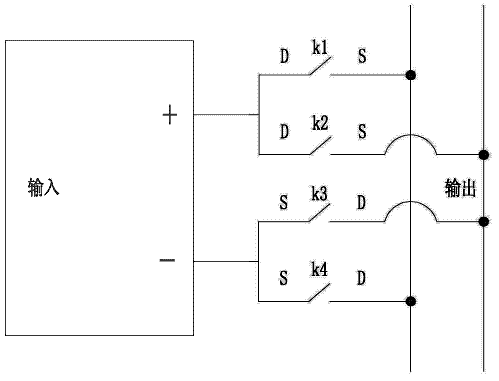
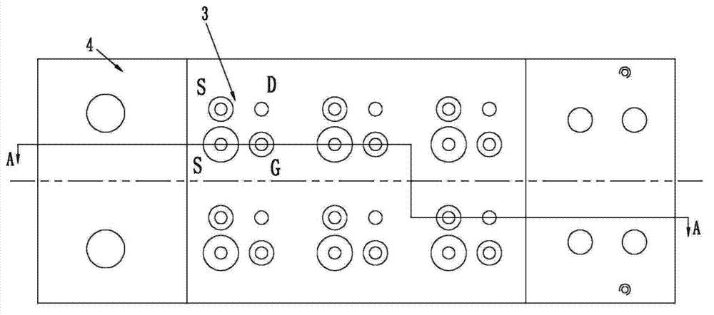
[0033] Such as Figure 2-6 As shown, a method for realizing balanced parallel connection of electronic switching devices includes:

[0034] (1) Connect the positive and negative inputs to two water-cooled busbars respectively to form a positive input water-cooled busbar and a negative input water-cooled busbar. The two water-cooled busbars are arranged in parallel; the water-cooled busbars are water-cooled aluminum busbars.

[0035] (2) Composite busbars are respectively arranged on the positive input water-cooled busbar and the negative input water-cooled busbar, wherein the composite busbar is composed of the same two layers of copper plates stacked alternately, and an insulating layer is set between the two layers of copper plates to insulate and isolate the two One-layer copper plate, the insulating layer is PET insulating paper; the two copper plates are respectively copper busbars, and the copper busbars are copper plates with opposite polarities after conducting electri...


PUM


Abstract

The invention discloses a method for realizing balanced parallel connection of electronic switching devices. The method comprises the following steps of: (1) connecting an anode input and a cathode input to two water-cooled bus bars to form an anode input water-cooled bus bar and a cathode input water-cooled bus bar; (2) overlapping two layers of same copper plates in a staggered way to construct a composite bus bar; (3) uniformly distributing a plurality of electronic switching devices on the overlapping region of the two layers of copper plates to construct electronic switching units; (4) arranging two groups of electronic switching units on the anode input water-cooled bus bar and the cathode water-cooled bus bar respectively, wherein the electronic switching devices of each group of electronic switching units are compressed against corresponding water-cooled bus bars; and (5) vertically connecting the drain and the source of each electronic switching device with a respective corresponding copper plate, and uniformly distributing each connecting point on the overlapping region of the copper plates to realize balanced parallel connection of the electronic switching devices. The invention further discloses a structure for realizing balanced parallel connection of electronic switching devices by using the method. Due to the adoption of the method and the structure, parallel electronic switching devices have higher current balancing properties and high heat dissipation rates.

Description

technical field [0001] The invention relates to a method for realizing balanced parallel connection of electronic switching devices, and also relates to a structure applying the method. Background technique [0002] In the power electronics industry, switching components are often used to control or transform electrical energy, such as insulated gate bipolar transistors (IGBTs) and power field effect transistors (mos tubes). This type of switching device is relatively fragile during operation. Overcurrent, high voltage, low voltage, unstable voltage, and high temperature will affect performance, life, and even cause damage. [0003] In order to meet the needs of large-capacity electrical equipment, parallel power electronic switching devices are usually used to control large currents, such as figure 1 shown. When connecting in parallel, it is very important to make each device flow an equal current. Once the current balance is destroyed, the device with too concentrated cu...

Claims


Application Information

Patent Timeline
Patent Type & Authority Applications(China)
IPC IPC(8): H03K17/567
Inventor 丁小松蔡小纯
Owner GUANGZHOU QINGTIAN INDAL
Why Eureka
Try Eureka