Vertical parasitic type precision navigation processor (PNP) device and manufacturing method thereof in bipolar complementary metal-oxide-semiconductor transistor (BiCMOS) technology

A vertical parasitic and process technology, applied in semiconductor/solid-state device manufacturing, electric solid-state devices, semiconductor devices, etc., can solve the problems of reduced device size, large device area, and large collector connection resistance, reducing area and large current. Amplification factor, the effect of reducing production cost

Active Publication Date: 2013-04-24
SHANGHAI HUAHONG GRACE SEMICON MFG CORP
View PDF3 Cites 0 Cited by
  • Summary
  • Abstract
  • Description
  • Claims
  • Application Information

AI Technical Summary

Problems solved by technology

The disadvantage is that the device area is large and the connection resistance of the collector is large
Since the extraction of the collector electrode in the prior art is realized through another active re

Method used


Image

  • Vertical parasitic type precision navigation processor (PNP) device and manufacturing method thereof in bipolar complementary metal-oxide-semiconductor transistor (BiCMOS) technology
  • Vertical parasitic type precision navigation processor (PNP) device and manufacturing method thereof in bipolar complementary metal-oxide-semiconductor transistor (BiCMOS) technology
  • Vertical parasitic type precision navigation processor (PNP) device and manufacturing method thereof in bipolar complementary metal-oxide-semiconductor transistor (BiCMOS) technology

Examples


Embodiment B

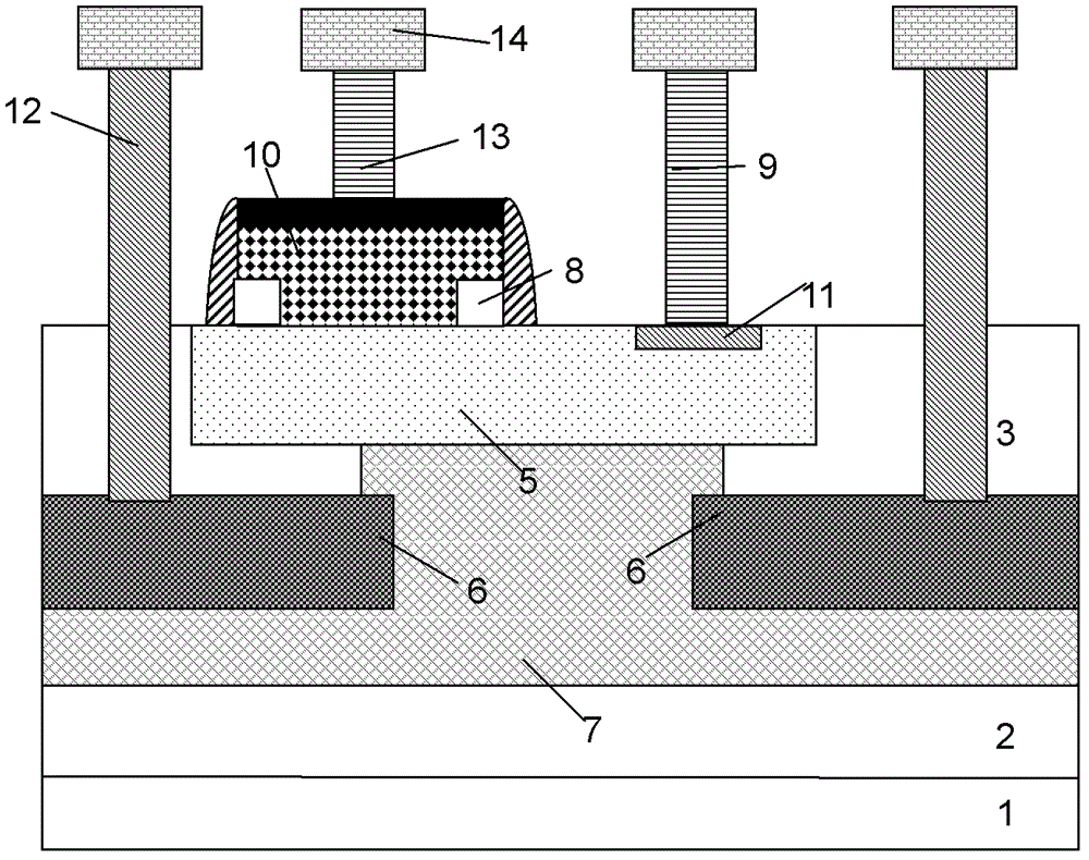
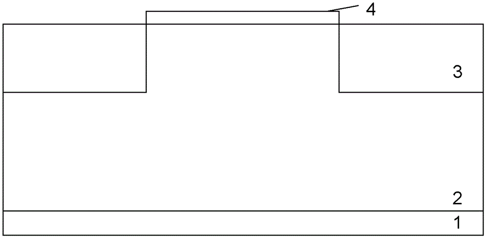
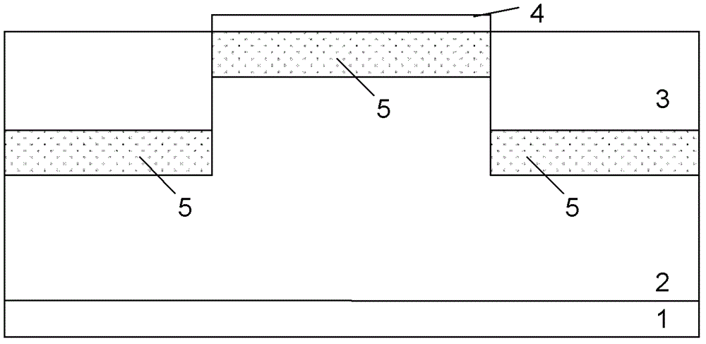
[0033] Such as figure 1 Shown is a schematic structural view of the vertical parasitic PNP device in the BiCMOS process of the embodiment of the present invention. The vertical parasitic PNP device in the BiCMOS process of the embodiment of the present invention is formed on a P-type silicon substrate 1 and placed on the P-type silicon substrate 1. An N-type deep well 2 is formed on a silicon substrate 1, and the active region is isolated by a shallow trench field oxygen 3, which is shallow trench isolation (STI). The vertical parasitic PNP device includes:

[0034] A collector region 7 is composed of a P-type ion implantation region formed in the active region, and the depth of the collector region 7 is greater than or equal to the depth of the bottom of the shallow trench field oxygen 3 . The process conditions of the P-type ion implantation region of the collector region 7 and the CMOS P well are the same, and the implantation impurity of the P-type ion implantation of the ...


PUM

PropertyMeasurementUnit
Thicknessaaaaaaaaaa

Abstract

The invention discloses a vertical parasitic type precision navigation processor (PNP) device in bipolar complementary metal-oxide-semiconductor transistor (BiCMOS) technology. The vertical parasitic type PNP device in the BiCMOS technology comprises a collector region, a base region, an emitter region and an artifact buried layer. The artifact buried layer is formed on the bottom of shallow groove field oxide on two sides of the collector region, expands horizontally into an active region and contacts with the collector region. A collector is led out by contacting with a deep hole which is formed in the shallow groove field oxide on the top of the artifact buried layer. The emitter region is constituted of P type polycrystalline silicon which is formed on the upper portion of the base region, and the emitter region is placed on one side which deviates from the active region. Metallic contact in the base region is placed on the other side of the active region. The invention further discloses a manufacturing method of the vertical parasitic type PNP device in the BiCMOS technology. The vertical parasitic type PNP device in the BiCMOS technology can be used as an output device in a high speed and high gain (HG) BiCMOS circuit, and thus one more device option is supplied to circuits, the area of the device can be effectively reduced, the collector resistance of a PNP tube is decreased, and the performance of the device is improved. By means of the manufacturing method of the vertical parasitic type PNP device in the BiCMOS technology, extra technological conditions are of no need, and production cost can be lowered.

Description

technical field [0001] The invention relates to the field of semiconductor integrated circuit manufacturing, in particular to a vertical parasitic PNP device in a BiCMOS process, and also relates to a method for manufacturing the vertical parasitic PNP device in the BiCMOS process. Background technique [0002] In RF applications, higher and higher device characteristic frequencies are required. In the BiCMOS process technology, NPN transistors, especially silicon-germanium heterojunction transistors (SiGe) or silicon-germanium carbon heterojunction transistors (SiGeC HBT) are good choices for UHF devices. And the SiGe process is basically compatible with the silicon process, so SiGe HBT has become one of the mainstreams of UHF devices. In this context, the requirements for the output device are correspondingly increased, such as having a certain current gain coefficient (not less than 15) and cut-off frequency. [0003] In the prior art, the output device can adopt a vert...

Claims


Application Information

Patent Timeline
IPC IPC(8): H01L23/528H01L29/06H01L29/732H01L21/331
Inventor 陈帆陈曦周正良陈雄斌潘嘉李昊薛凯周克然蔡莹
Owner SHANGHAI HUAHONG GRACE SEMICON MFG CORP
Why Eureka
Try Eureka