Shift register cell, gate driving circuit, data driving circuit and display

A shift register and drive control technology, which is applied in the field of gate drive circuits, data drive circuits and shift register units, can solve the problems of reducing circuit operating speed, slow circuit operating speed, and degradation of transistor device characteristics, so as to reduce design Effects of complexity, increased operating speed, and reduced rise time

Active Publication Date: 2013-05-01
PEKING UNIV SHENZHEN GRADUATE SCHOOL
View PDF4 Cites 61 Cited by
  • Summary
  • Abstract
  • Description
  • Claims
  • Application Information

AI Technical Summary

Problems solved by technology

In some previously reported circuit schemes, the working speed of the shift register unit is slow, although it can meet the requirements of the gate drive circuit, it is not conducive to the realization of high-speed data drive circuit
There are two main reasons: on the one hand, the driving transistor is usually only used as a charging transistor, and the reduction of the falling delay time of the output signal can only be achieved by increasing the size of the discharging transistor, which cannot take into account the working speed and layout area of ​​the circuit; on the other hand Although the bootstrap technology is used to improve the driving ability of the driving transistor, due to the possible functional conflicts between the modules of the circuit, the shift register unit has a transistor leakage phenomenon during normal operation, which reduces the working speed of the circuit.
In addition, in order to suppress the clock feedthrough effect and ensure the stability of the low-level output signal, the existing circuit design usually has high design complexity and low yield, and there are also serious degradation of individual transistor device characteristics and short circuit working life. Shortcomings
[0004] figure 1 Shown is a circuit diagram of a disclosed shift register unit for a gate drive circuit that requires ten transistors Q 1 -Q 10 , and a capacitor C 1 , the working speed of the circuit is slow, the design is complicated, and some transistors are subjected to high voltage stress, which affects the working life of the circuit

Method used


Image

  • Shift register cell, gate driving circuit, data driving circuit and display
  • Shift register cell, gate driving circuit, data driving circuit and display
  • Shift register cell, gate driving circuit, data driving circuit and display

Examples


Embodiment 1

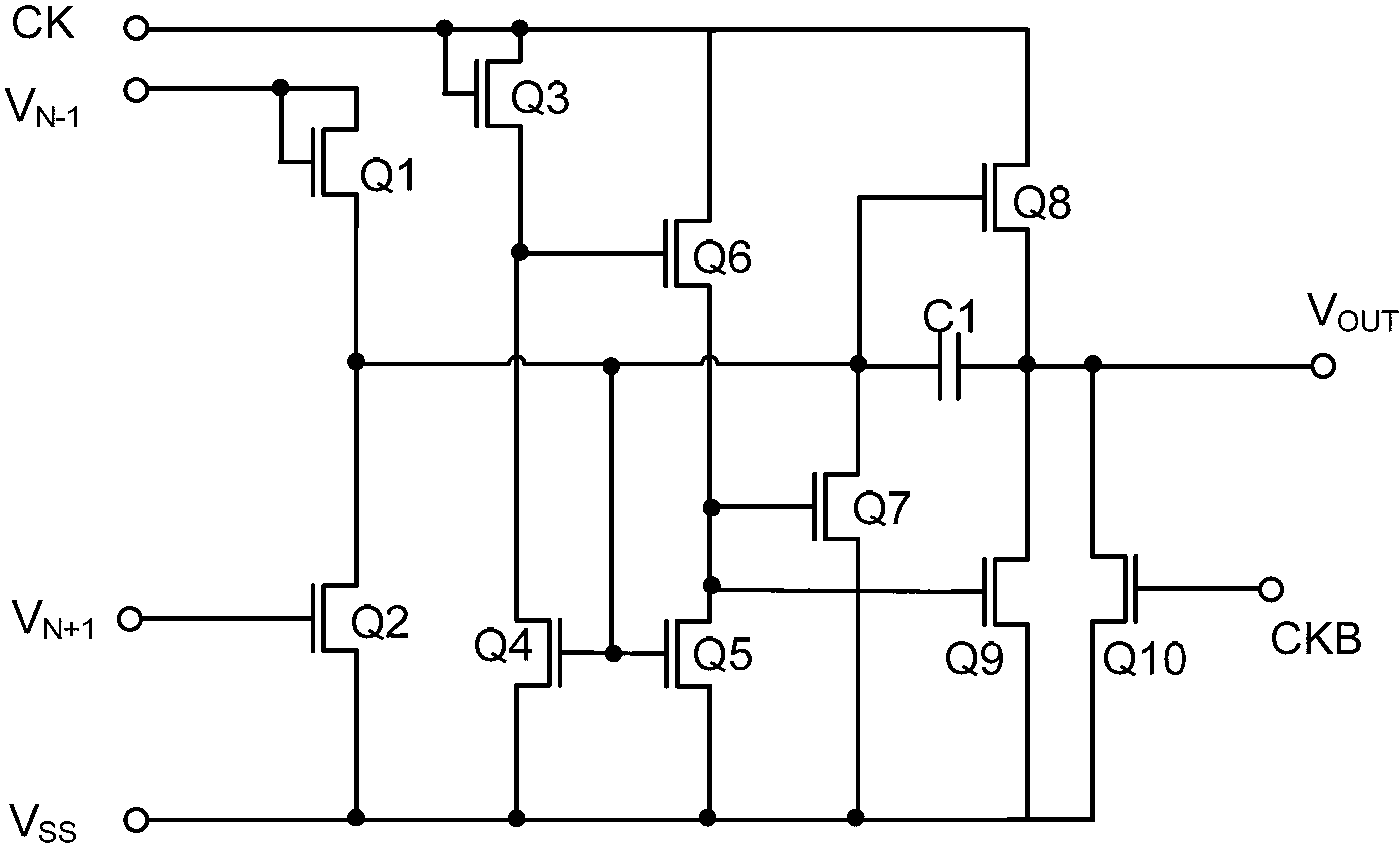
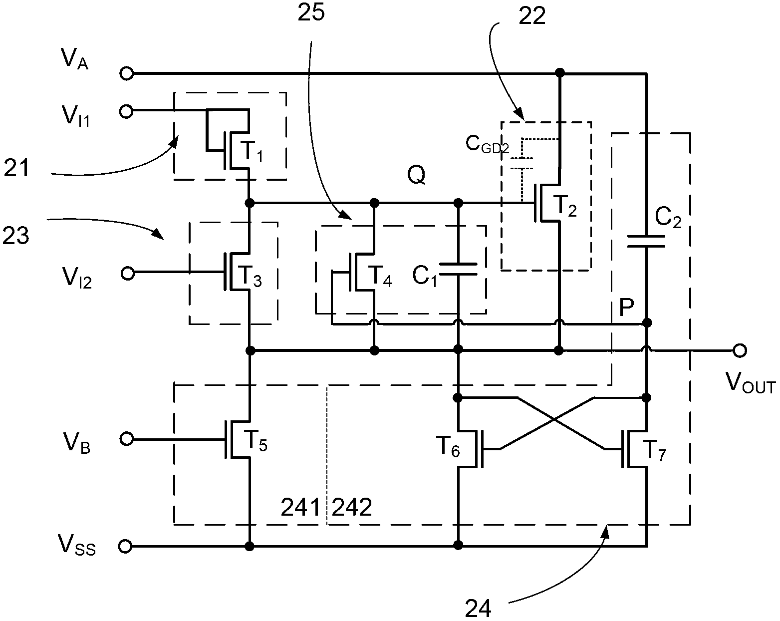
[0055] The shift register unit is a very important unit circuit to realize the gate drive circuit and the data drive circuit. Take the shift register unit as an example, such as image 3 As shown, the shift register unit of this embodiment includes an input module 21 , a driver module 22 , a driver control terminal pull-down delay module 23 , a clock feedthrough suppression module 25 and a low level maintenance module 24 .

[0056] The signal input end of the input module 21 is connected to the first signal input end, and the first pulse signal V is input. I1 ; The clock input end of the driving module 22 is connected to the first clock signal input end, and the first clock signal V is input A , the drive module 22 has a drive control terminal Q, the output terminal of the input module 21 is connected to the drive control terminal of the drive module 22, and the input module 21 is used to receive the first pulse signal V from the first signal input terminal I1 , to provide a ...

Embodiment 2

[0106] like Figure 9 Shown is a circuit diagram of a second embodiment of a shift register unit. Compared with the first embodiment of the shift register unit, the circuit in this embodiment adopts the same clock feedthrough control module 25, including a small-sized fourteenth transistor T 14 and the eleventh capacitor C 11 , but the fourteenth transistor T 14 Using a conventional connection: the fourteenth transistor T 14 The control pole of is coupled to the first signal input terminal, and its first pole (such as the drain) and second pole (such as the source) are respectively coupled to the drive control terminal Q and the signal output terminal V OUT ; Eleventh capacitor C 11 Coupled to the drive control terminal Q and the signal output terminal V OUT between. In the non-selection stage of the shift register unit, when the first clock signal V A When the level is high, the fourteenth transistor T 14 Turn on and release the coupling charge of the driving control ...

Embodiment 3

[0111] like Figure 10 Shown is a circuit diagram of the shift register unit of the third embodiment. Compared with Embodiment 1 or 2 of the shift register unit, a pull-down unit 26 is added in the circuit of this embodiment, including a transistor T 8 . Transistor T 8 The control pole of is connected to the second signal input terminal and responds to the second pulse signal V B , whose first pole (such as drain) and second pole (such as source) are respectively coupled to the signal output terminal V OUT with a low potential source V SS . In this embodiment, the working process of the shift register unit is basically the same as that of Embodiment 1 of the shift register unit, and will not be repeated here. The difference is that during the pull-down process of the shift register unit, the eighth transistor T 8 conduction, the signal output terminal V OUT can also be turned on by the transistor T 8 Discharge; therefore, the falling time of the output signal can be f...


PUM


Abstract

The invention discloses a shift register cell, a gate driving circuit, a data driving circuit and a display, wherein the shift register cell comprises a first signal input end, a second signal input end, a first clock signal input end, a pull-down control signal input end, a signal output end (VOUT), an input module (21), a driving module (22), a driving control end pull-down delay module (23), a clock feed through inhibition module (25) and a low-level retention module (24). According to the invention, the signal output end can quickly discharge by a charging transistor in the driving module by prolonging discharging time for a driving control end in the shift register cell; and the electricity leakage of the transistor in the clock feed through inhibition module is inhibited, so that work speed and integration degree of the circuit are improved.

Description

technical field [0001] The present application relates to a display, in particular to a gate driving circuit, a data driving circuit and a shift register unit of the display. Background technique [0002] Active flat panel display has become the mainstream technology in the field of modern display. In an active flat panel display, the gate drive circuit and the data drive circuit are very important components. The traditional method is to connect the peripheral drive IC to the display panel by pressing and sealing. In recent years, integrated display driving circuits have gradually become a research hotspot in flat panel display technology. The so-called integrated display drive circuit mainly includes two parts: an integrated gate drive circuit and an integrated data drive circuit, which means that the gate drive circuit and data drive circuit are fabricated on the display panel together with pixel TFTs in the form of thin film transistors (TFTs). Compared with the tradit...

Claims


Application Information

Patent Timeline
Patent Type & Authority Applications(China)
IPC IPC(8): G09G3/36G11C19/28
Inventor 张盛东胡治晋廖聪维
Owner PEKING UNIV SHENZHEN GRADUATE SCHOOL
Why Eureka
Try Eureka