
Apparatus and method for carrying out selenylation treatment on CIGS (copper indium gallium selenide) thin films and CIGS thin-film device
A technology of a copper indium gallium selenide and a processing device, which is applied in the field of copper indium gallium selenide thin film devices, can solve the problems that the thin film is prone to pinholes, the selenium vapor pressure is not stable enough, and cannot be processed in batches, so as to achieve stable selenization process and prevent high temperature Oxidation to ensure repeatable effect
- Summary
- Abstract
- Description
- Claims
- Application Information
AI Technical Summary
Problems solved by technology
Method used
Image

Examples
Embodiment 1
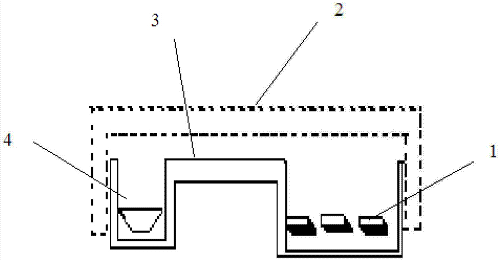
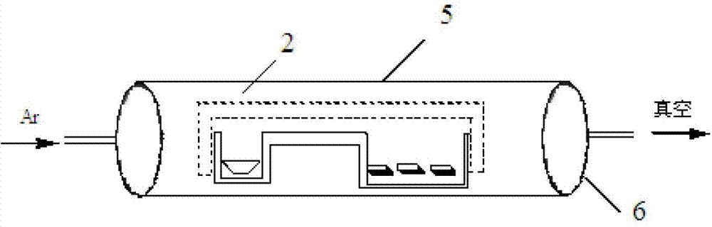
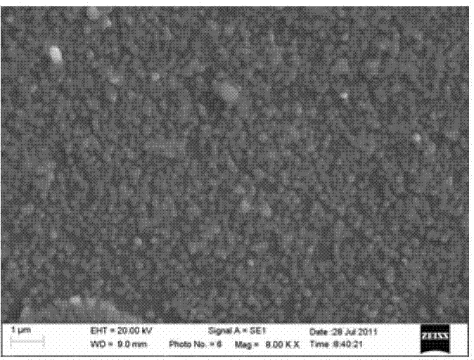
[0054] Place the crucible with selenium powder and a CIGS film to be treated in the selenium source groove 4 and the CIGS film groove 1 of the closed selenization unit respectively, and the selenization unit is placed in the electronic temperature-controlled dual temperature zone In the quartz tube 5 of the tubular heating furnace, turn on the vacuum pump, evacuate to 0.4Pa, close the vacuum valve, then open the high-purity nitrogen valve, feed high-purity nitrogen, keep the nitrogen pressure at 40Pa, open the heating switch of the tubular heating furnace, Control the temperature in the selenium source area to 180°C, and control the temperature in the CIGS thin film area to 400°C. Keep the temperature and nitrogen pressure, selenize for 60 minutes, then stop heating, slowly cool down, take out the CIGS thin film device, and perform characterization. The SEM image is as follows figure 1 As shown, the XRD pattern is as Image 6 Shown, as the XRD spectrum before the contrast sele...
Embodiment 2
[0056] Place the crucible containing the selenium powder and the two CIGS films to be treated in the selenium source groove 4 and the CIGS film groove 1 of the closed selenization unit respectively, and the selenization unit is placed in an electronic temperature-controlled dual-temperature In the quartz tube 5 of the district tubular heating furnace, turn on the vacuum pump, evacuate to 0.4Pa, close the vacuum valve, then open the high-purity nitrogen valve, feed high-purity nitrogen, keep the nitrogen pressure at 150Pa, and turn on the heating switch of the tubular heating furnace , control the temperature in the selenium source area to 190°C, and control the temperature in the CIGS thin film area to 400°C. Maintain the temperature and nitrogen pressure, selenize for 60 minutes, then stop heating, slowly cool down, and take out the CIGS thin film device for characterization.
Embodiment 3
[0058] Place the crucible containing the selenium powder and the four CIGS films to be treated in the selenium source groove 4 and the CIGS film groove 1 of the closed selenization unit respectively, and the selenization unit is placed in an electronic temperature-controlled dual-temperature In the quartz tube 5 of the district tubular heating furnace, turn on the vacuum pump, evacuate to 0.6Pa, close the vacuum valve, then open the high-purity argon valve, feed high-purity argon, keep the argon pressure at 80Pa, and turn on the tubular heating Furnace heating switch, control temperature of selenium source area to 210°C, control temperature of CIGS device area to 500°C, maintain temperature and nitrogen pressure, selenization treatment for 55min, then stop heating, slowly cool down, take out CIGS thin film device for characterization.
PUM
 Abstract
Description
Claims
Application Information