Method and device for photoresist coating

A photoresist and coating technology, which is applied in the direction of photo-engraving process coating equipment, electrical components, semiconductor/solid-state device manufacturing, etc. The effect of improving the uniformity of resistance thickness, reducing the defect rate, and solving the problem of over-etching of the protective layer

Inactive Publication Date: 2016-01-13
PEKING UNIV FOUNDER GRP CO LTD +1
View PDF3 Cites 0 Cited by
  • Summary
  • Abstract
  • Description
  • Claims
  • Application Information

AI Technical Summary

Problems solved by technology

[0003] Generally, the production of a semiconductor device requires multiple photolithography processes. The wafer undergoes the front-end production process, and the corresponding circuit layout is etched on the wafer, resulting in uneven surface of the wafer. Photoresist coating is performed on uneven wafer surfaces, resulting in uneven thickness of photoresist in each area of ​​the wafer surface
[0004] Among them, the thickness of the photoresist coated on the sidewall area of ​​the groove will be relatively thin. When the thickness is lower than a certain threshold, the remaining photoresist will not be able to resist etching after exposure and development. Define The circuit is damaged, causing the chip not to work properly

Method used


Image

  • Method and device for photoresist coating
  • Method and device for photoresist coating
  • Method and device for photoresist coating

Examples


Embodiment Construction

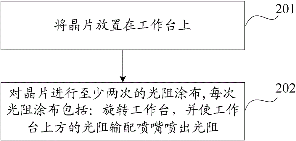
[0018] In the embodiment of the present invention, when carrying out photoresist coating to uneven wafer surface, carry out two times, three times, or multiple photoresist coatings, the thickness of the photoresist coated in groove area like this can be thickened, avoids concave The thickness of the photoresist coated on the sidewall area of ​​the groove is not enough to resist etching and cannot protect the circuit.

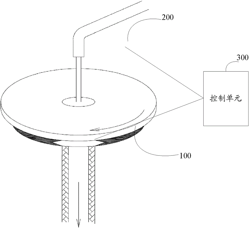
[0019] The photoresist coating process generally adopts the center selective spraying method, and the photoresist coating device such as figure 1 As shown, it includes: a workbench 100 , a photoresist delivery and distribution nozzle 200 and a control unit 300 . in,

[0020] The workbench 100 is used to place wafers, and can be rotated under the control of the control unit 300 , generally the control unit 300 controls the rotation speed of the workbench 100 .

[0021] The photoresist delivery and distribution nozzle 200 is located above the workbench 100 and c...


PUM


Abstract

The invention discloses a method and a device for photoresist coating. The method and the device for the photoresist coating are used for reducing reject ratio of semiconductor chips. The method for the photoresist coating includes the following steps: placing a wafer on a working table, and conducting at least twice of photoresist coating to the wafer. Each time of photoresist coating comprises steps: rotating the working table, and enabling a photoresist transmission and distribution nozzle above the working table to erupt photoresistance. Thus, photoresist thickness uniformity of coating can be markedly improved, photoresist residual thickness at the thinnest position after etching is enough to block protection layer etching, and therefore the problem of over etching of a protection layer is solved, pattern definition integrity after etching is ensured, and reject rate of semiconductor chips is reduced.

Description

technical field [0001] The invention relates to the technical field of semiconductor device production, in particular to a photoresist coating method and device. Background technique [0002] At present, semiconductor devices are manufactured using a photolithography (MASK) process, and the photolithography process includes: photoresist coating, masking, exposure, development, etching and stripping. Specifically, it includes: uniformly coating the photoresist on the surface of the chip, so that the chip can be patterned by an exposure machine, and the circuit is defined after etching. [0003] Generally, the production of a semiconductor device requires multiple photolithography processes. The wafer undergoes the front-end production process, and the corresponding circuit layout is etched on the wafer, resulting in uneven surface of the wafer. Photoresist coating is performed on uneven wafer surfaces, resulting in uneven photoresist thickness in each area of ​​the wafer sur...

Claims


Application Information

Patent Timeline
Patent Type & Authority Patents(China)
IPC IPC(8): H01L21/312G03F7/16
Inventor 戴新华彭超群方表峰杜兆董
Owner PEKING UNIV FOUNDER GRP CO LTD
Why Eureka
Try Eureka