Structure and manufacturing method of dual-channel high-voltage junction field effect transistor for reducing pinch-off voltage

A field effect transistor and pinch-off voltage technology, which is applied in the field of semiconductor integrated circuits, can solve the problem of high pinch-off voltage, and achieve the effect of reducing the pinch-off voltage and easy depletion.

Active Publication Date: 2015-10-14
SHANGHAI HUAHONG GRACE SEMICON MFG CORP
View PDF3 Cites 0 Cited by
  • Summary
  • Abstract
  • Description
  • Claims
  • Application Information

AI Technical Summary

Problems solved by technology

[0002] The channel region of the current high-voltage JFET device is an N or P-type single channel, and the pinch-off voltage is relatively high.
like figure 1 As shown, the channel region of a traditional HV N-channel JFET device is composed of a DNW N-type impurity, which has only one current channel, which is not easy to be depleted

Method used


Image

  • Structure and manufacturing method of dual-channel high-voltage junction field effect transistor for reducing pinch-off voltage
  • Structure and manufacturing method of dual-channel high-voltage junction field effect transistor for reducing pinch-off voltage
  • Structure and manufacturing method of dual-channel high-voltage junction field effect transistor for reducing pinch-off voltage

Examples


Embodiment Construction

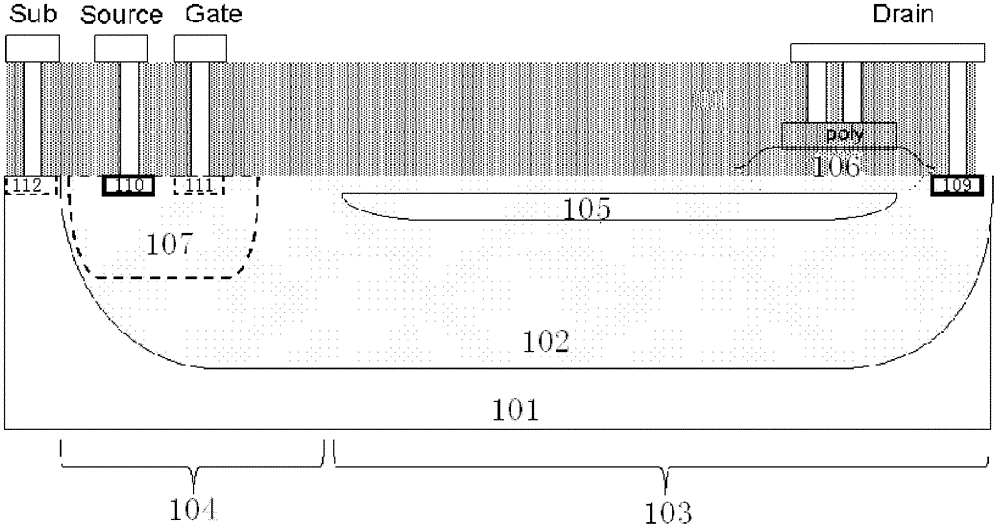
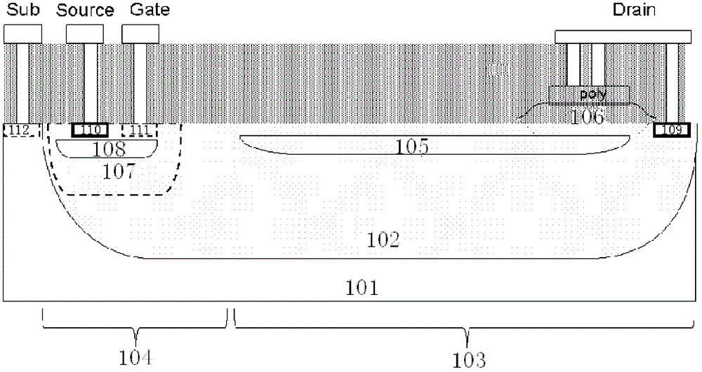
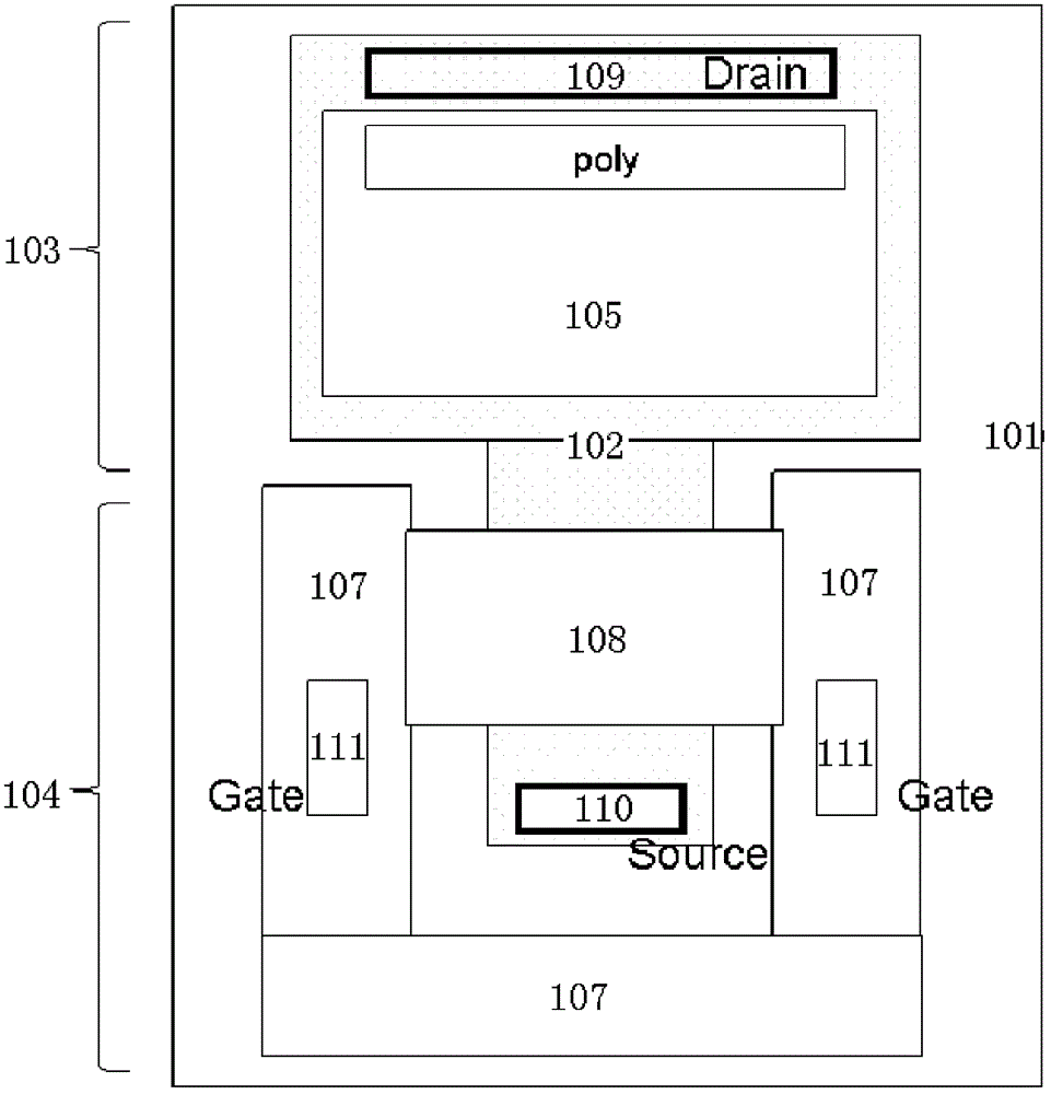
[0022] The double-channel high-voltage junction field effect transistor of the present invention reduces the structure of the pinch-off voltage, such as figure 2 As shown, a well region 102 having a second conductivity type opposite to the first conductivity type is formed on a silicon substrate 101 having a first conductivity type, and the well region 102 has a drift region 103 and a body region 104, wherein The drift region 103 is used for high voltage resistance, and the body region 104 is the channel region of the JFET. A drift region inversion layer 105 having a first conductivity type is formed in the drift region 103 , and an isolation structure 106 is formed above one end of the drift region inversion layer 105 . A gate region 107 of the first conductivity type is formed outside the channel region 104, and a channel region inversion layer 108 of the first conductivity type is formed in the channel region 104, such as image 3 , Figure 4 As shown, the channel region...


PUM


Abstract

The invention discloses a pinch-off voltage reducing structure of a dual-channel high voltage junction field effect transistor (FET) and a manufacturing method of the pinch-off voltage reducing structure of the dual-channel high voltage junction FET. A well region provided with a channel region and a drift region is formed in a silicon substrate, a drift region inversion layer is arranged in the drift region, a gate region is formed on the outer side of the channel region, a channel region inversion layer is arranged in the channel region, the transverse width of the channel region inversion layer is longer than the transverse width of the channel region, and two ends of the channel region inversion layer are connected with the gate region. A drain electrode leading-out terminal is formed in the drift region, a source electrode leading-out terminal is formed in the channel region, a gate electrode leading-out terminal is formed in the gate region, and a substrate leading-out terminal is formed in the substrate region. The drift region, the drain electrode leading-out terminal and the source electrode leading-out terminal are in a second conductivity type, the substrate, the drift region inversion layer, the channel region inversion layer, the gate region, the gate leading-out terminal and the substrate leading-out terminal are in a first conductivity type, and electrodes are led out from the leading-out terminals. According to the pinch-off voltage reducing structure of the dual-channel high voltage junction FET and the manufacturing method of the pinch-off voltage reducing structure of the dual-channel high voltage junction FET, impurities which are opposite in type are implanted inside the channel region to form double channels, namely an upper channel and a lower channel, the opposite impurities are arranged in the channel region at the same time, and therefore each channel can be exhausted more easily, and pinch-off voltage is lowered.

Description

technical field [0001] The invention relates to the field of semiconductor integrated circuits, in particular to a structure for reducing the pinch-off voltage of a double-channel high-voltage junction field effect transistor. The invention also relates to a manufacturing method of the dual-channel high-voltage junction field effect transistor. Background technique [0002] The channel region of the current high-voltage JFET device is an N or P-type single channel, and the pinch-off voltage is relatively high. Such as figure 1 As shown, the channel region of a traditional HV N-channel JFET device is composed of a DNW N-type impurity, and there is only one current channel, which is not easy to be depleted. Contents of the invention [0003] The technical problem to be solved by the present invention is to provide a structure for reducing the pinch-off voltage of a dual-channel high-voltage junction field effect transistor, which can reduce the pinch-off voltage of the jun...

Claims


Application Information

Patent Timeline
Patent Type & Authority Patents(China)
IPC IPC(8): H01L29/10H01L29/808H01L21/337
Inventor 宁开明
Owner SHANGHAI HUAHONG GRACE SEMICON MFG CORP
Why Eureka
Try Eureka