Point contact Laterally Diffused Metal Oxide Semiconductor (LDMOS) structure transistor unit

A technology of transistor unit and point contact, which is applied in the direction of transistors, electrical components, semiconductor devices, etc., and can solve the problems such as the difficulty of further reducing the drain-source PN junction capacitance, the limitation of broadband microwave high-power applications of devices, and the large chip area of ​​high-power devices. , to achieve the effect of satisfying broadband, reducing thermal resistance and dispersing heat source

Inactive Publication Date: 2011-07-27
NO 55 INST CHINA ELECTRONIC SCI & TECHNOLOGYGROUP CO LTD
View PDF0 Cites 0 Cited by
  • Summary
  • Abstract
  • Description
  • Claims
  • Application Information

AI Technical Summary

Problems solved by technology

Due to the limitation of the breakdown voltage, the width of the drift region between the channel and the drain contact window cannot be reduced, so it is difficult to further reduce the drain-source PN junction capacitance between the drift region and the drain contact region and the substrate in the rectangular strip transistor unit
Therefore, the area of ​​the high-power device chip is often relatively large, and the drain-source PN junction capacitance is also relatively large, which limits the application of broadband microwave high-power devices

Method used


Image

  • Point contact Laterally Diffused Metal Oxide Semiconductor (LDMOS) structure transistor unit
  • Point contact Laterally Diffused Metal Oxide Semiconductor (LDMOS) structure transistor unit
  • Point contact Laterally Diffused Metal Oxide Semiconductor (LDMOS) structure transistor unit

Examples


Embodiment Construction

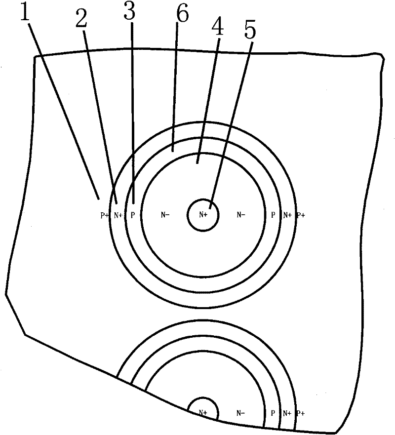
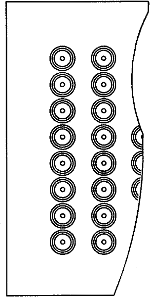
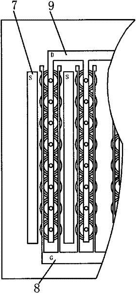
[0013] Control attached figure 1 , its structure is a point-contact LDMOS structure transistor unit, its structure is that the N+ doped drain region 5 is a circle or a regular polygon, forming a drain contact region; the periphery of the N+ doped drain region 5 is surrounded by an N-doped drift region 4; -The periphery of the doped drift region 4 is surrounded by a P-type doped channel region 3, and above the P-type doped channel region 3 is an N+ doped polysilicon gate 6; between the P-type doped channel region 3 and the N+ doped polysilicon gate 6 are separated by a silicon dioxide insulating layer; the P-type doped channel region 3 is surrounded by an N+ doped source region 2; the N+ doped source region 2 is surrounded by a P+ doped source region 1, and the P+ doped source region 1 The doping depth exceeds the thickness of the epitaxial layer, and the P+ doping source region 1 is connected to the P+ substrate; the P+ doping source region 1 and the N+ doping source region 2...


PUM


Abstract

The invention relates to a point contact Laterally Diffused Metal Oxide Semiconductor (LDMOS) structure transistor unit. The drain contact region of the transistor unit is designed to be a round or an equilateral polygon. The region is in the center of the unit and is surrounded by drift region, channel region and source region successively. The area ratio of grid width to the junction area of drain-source PN is twice as high as regular LDMOS. The transistor units constitute the chip of the device in the directions of X and Y periodically. The invention has the advantages that the point contact LDMOS structure transistor unit can effectively disperse heat source, reduce thermal resistance, and enhance the working bandwidth, transmission gain, power and other performance indexes of the device.

Description

technical field [0001] The invention relates to a point-contact LDMOS structure transistor unit suitable for the production of microwave power transistors, and belongs to the technical field of semiconductor microelectronics design and manufacture. Background technique [0002] At present, the existing lateral double-diffused metal oxide transistor (LDMOS) units are usually in a rectangular strip structure, and the transistor units are distributed along the long sides of the rectangle according to a certain period to form a device chip. In order to improve the microwave performance of the device chip, it is usually necessary to reduce electrical parameters such as parasitic capacitance and parasitic inductance. The main measures taken in device design and manufacture include: using concentrated boron doped (P+) substrate; light boron doped epitaxial layer (P-); concentrated boron doped (P+) back source; submicron-sized short channel; Depletion of the drift region, etc.; in ...

Claims


Application Information

Patent Timeline
Patent Type & Authority Patents(China)
IPC IPC(8): H01L29/78H01L29/417H01L29/06H01L29/10H01L27/088
Inventor 傅义珠
Owner NO 55 INST CHINA ELECTRONIC SCI & TECHNOLOGYGROUP CO LTD
Why Eureka
Try Eureka