Shield gate groove type field effect transistor with low on-resistance and preparation method thereof

A field effect transistor, low on-resistance technology, applied in the field of shielded gate trench type field effect transistor and its preparation, can solve the problem of high peak voltage, achieve the effect of improving switching speed and easy depletion

Pending Publication Date: 2022-07-12
无锡先瞳半导体科技有限公司
View PDF0 Cites 0 Cited by
  • Summary
  • Abstract
  • Description
  • Claims
  • Application Information

AI Technical Summary

Problems solved by technology

[0004] In the SGT device, due to the electric field concentration effect and the high doping concentration of polysilicon in the shield gate, when the SGT device is forward-blocked, the charge flux emitted by the ionized dono

Method used


Image

  • Shield gate groove type field effect transistor with low on-resistance and preparation method thereof
  • Shield gate groove type field effect transistor with low on-resistance and preparation method thereof
  • Shield gate groove type field effect transistor with low on-resistance and preparation method thereof

Examples


Example Embodiment

[0051] Example 1

[0052] In the SGT device, due to the electric field concentration effect and the high polysilicon doping concentration of the shielding gate, when the SGT device is blocked in the forward direction, the parasitic capacitance formed between the shielding gate and the substrate region is large, which reduces the switching speed of the transistor. .

[0053]Therefore, in order to improve the switching speed of the SGT device, the parasitic capacitance formed between the shielding gate and the substrate region needs to be weakened. Embodiments of the present application provide a shielded gate trench field effect transistor with low on-resistance.

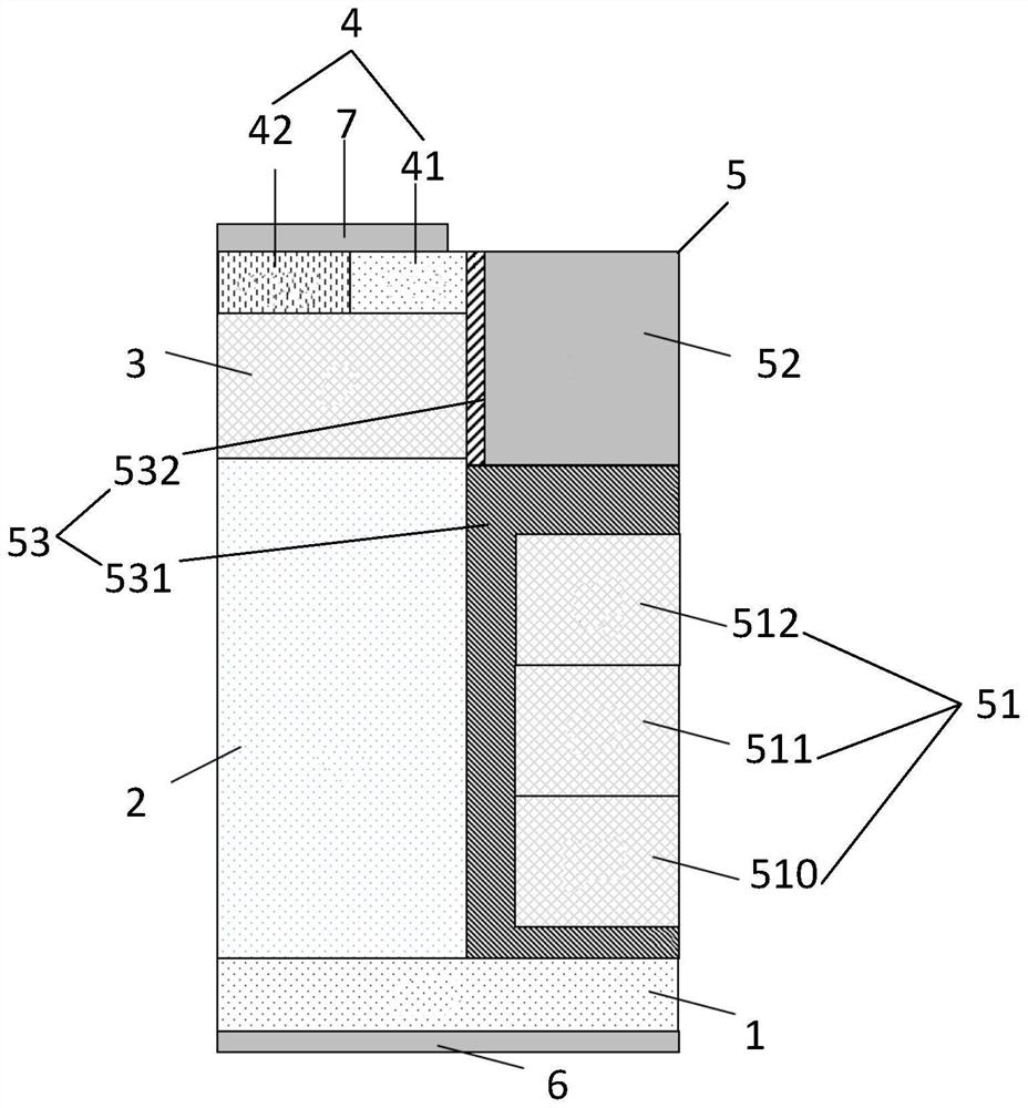
[0054] figure 1 It is a schematic structural diagram of the shielded gate trench field effect transistor with low on-resistance shown in the embodiment of the present application.

[0055] see figure 1 , the shielded gate trench field effect transistor with low on-resistance shown in the embodiment of the present...

Example Embodiment

[0069] Embodiment 2

[0070] Based on the transistor described in the first embodiment, due to the electric field concentration effect, when the SGT device is blocked in the forward direction, the electric charge and electric flux emitted by the ionization donor in the withstand voltage region are concentrated at the corner of the shield gate in the trench region, resulting in the channel The corners of the trench gates experience higher peak voltages.

[0071] Therefore, in order to improve the withstand voltage capability of the SGT device, it is necessary to weaken the electric field strength at the corners of the shield gate in the trench region. Embodiments of the present application provide a shielded gate trench field effect transistor with low on-resistance.

[0072] figure 1 It is a schematic structural diagram of the shielded gate trench field effect transistor with low on-resistance shown in the embodiment of the present application.

[0073] see figure 1 , the ...

Example Embodiment

[0086] Embodiment 3

[0087] Corresponding to the shielded-gate trench field effect transistor with low on-resistance shown in the first embodiment, the present application also provides a method for preparing a shielded-gate trench field-effect transistor with low on-resistance and the corresponding Example.

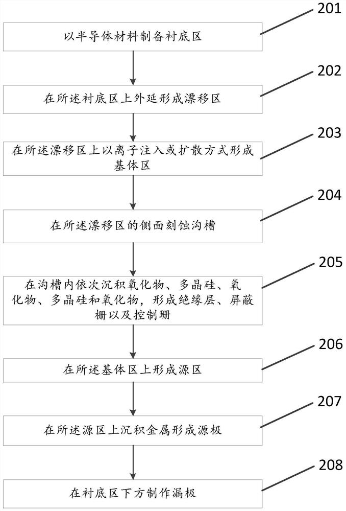
[0088] figure 2 It is a schematic flowchart of a method for fabricating a shielded gate trench field effect transistor according to an embodiment of the present application.

[0089] like figure 2 As shown, the method for fabricating the shielded gate trench field effect transistor with low on-resistance shown in the embodiment of the present application includes the following steps:

[0090] 201. Prepare a substrate region with a semiconductor material;

[0091] In the embodiment of the present application, the substrate region is prepared with N-type heavily doped semiconductor material, that is, the doping type of the substrate region is N-type doping, and the ...


PUM


Abstract

The invention relates to a shield gate trench field effect transistor with low on-resistance. The shield gate trench field effect transistor comprises a substrate region, a drift region, a matrix region, a source region, a trench region, a drain electrode and a source electrode, the trench region comprises a shield gate, a control gate, an insulating layer and a metal gate; the shielding grid is of a variable doping concentration structure, and the doping concentration of the shielding grid is gradually reduced from top to bottom. When the transistor is blocked in the forward direction, the doping concentration of the part, close to the substrate area, of the shielding grid is low. Therefore, the part, close to the substrate area, of the shielding grid is easier to deplete under the same external voltage, namely, the part close to the substrate area has a thicker depletion layer width. The width of the depletion layer is inversely proportional to the capacitance of the stray capacitance, so that the stray capacitance formed between the shield gate and the substrate region is smaller, the stray capacitance formed between the shield gate and the substrate region is weakened, and the switching speed of the device is further improved.

Description

technical field [0001] The present application relates to the technical field of power semiconductor devices, and in particular, to a shielded gate trench field effect transistor with low on-resistance and a preparation method thereof. Background technique [0002] Shielded gate trench field effect transistors (Split Gate Trench, SGT) have been widely used in important low-voltage fields such as power management. SGT has high channel density and good charge compensation effect. In addition, the shielded gate structure effectively isolates the coupling between the control gate and the drain, thereby significantly reducing the transfer capacitance. [0003] Therefore, SGT has lower specific on-resistance, smaller conduction and switching losses, and higher operating frequency. [0004] In the SGT device, due to the electric field concentration effect and the high polysilicon doping concentration of the shielding gate, when the SGT device is blocked in the forward direction, ...

Claims


Application Information

Patent Timeline
IPC IPC(8): H01L29/49H01L29/78H01L21/336
CPCH01L29/4916H01L29/7813H01L29/66734
Inventor 张子敏王宇澄虞国新吴飞钟军满
Owner 无锡先瞳半导体科技有限公司
Why Eureka
Try Eureka