Solder resisting method for circuit board

A circuit board and solder mask technology, applied in the field of circuit board solder mask, can solve the problems that the production plan cannot be achieved normally, is not suitable for mass processing, and the printing process is complicated. Effect

Inactive Publication Date: 2013-05-08
SHENNAN CIRCUITS
View PDF5 Cites 30 Cited by
  • Summary
  • Abstract
  • Description
  • Claims
  • Application Information

AI Technical Summary

Problems solved by technology

[0020] The above-mentioned processing methods have the following problems: 1. Single-sided silk screen printing plus manual suction holes have the risk of holes not being sucked clean, and require a lot of manpower, which is not

Method used


Image

  • Solder resisting method for circuit board
  • Solder resisting method for circuit board
  • Solder resisting method for circuit board

Examples


Embodiment Construction

[0043] In order to describe the technical content, structural features, achieved goals and effects of the present invention in detail, the following will be described in detail in conjunction with the embodiments and accompanying drawings.

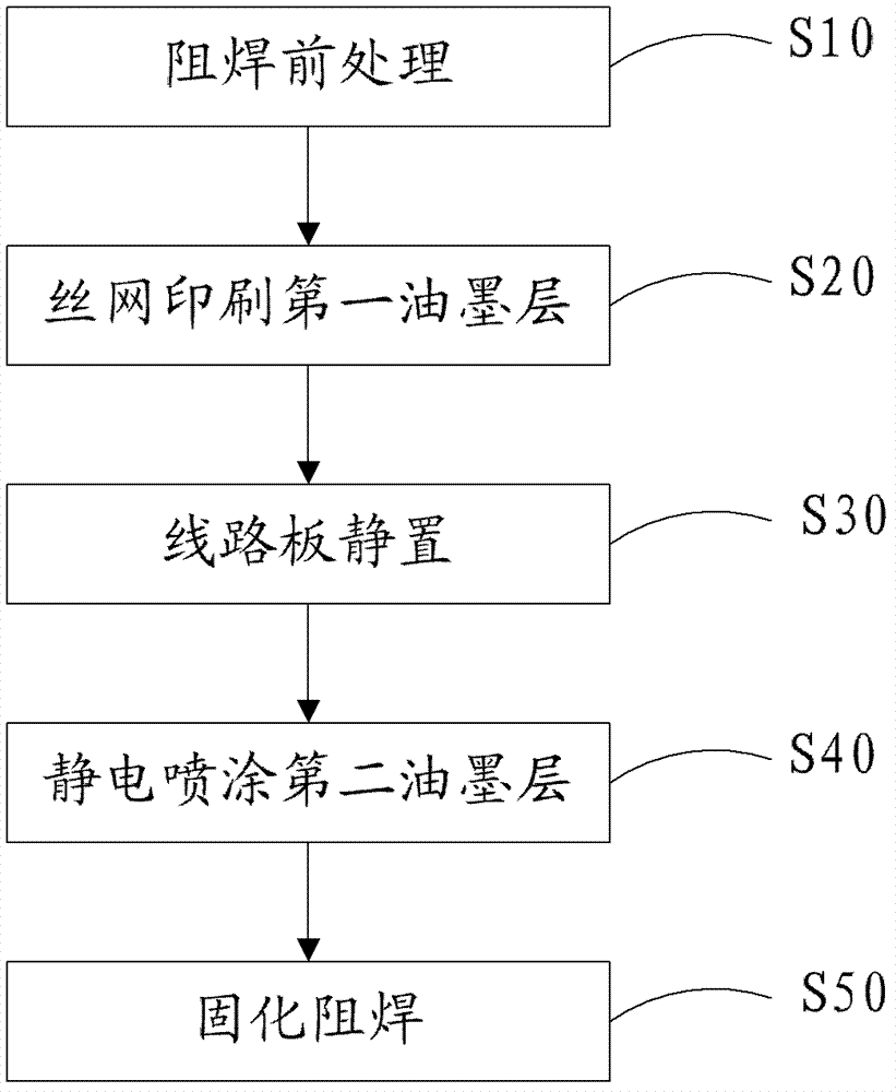
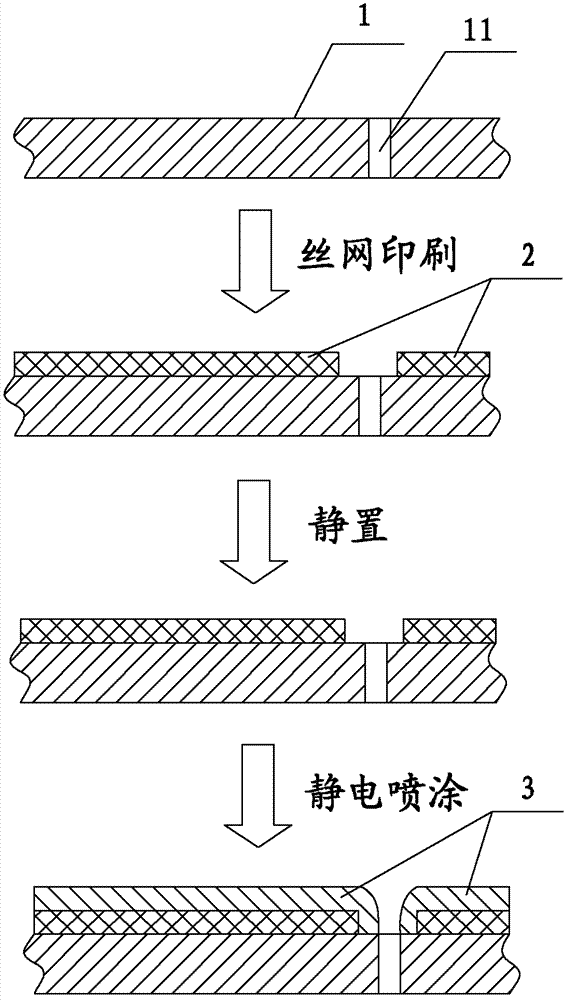
[0044] see figure 1 as well as figure 2 , the invention provides a circuit board solder resist method, comprising steps:

[0045]S10: Pre-treatment of solder resist: Specifically, the circuit board 1 is ground with volcanic ash, the abrasive concentration is 10%-15% (volume), and the width of the grinding scar is 10-14mm. This step is mainly to clean and roughen the surface of the circuit board 1 so that the solder resist ink can have a better bonding force with the circuit board and prevent the solder resist layer from falling off. If the surface of the circuit board is clean enough and the copper surface is rough enough before the solder mask is processed, the step of pre-solder mask treatment can also be omitted.

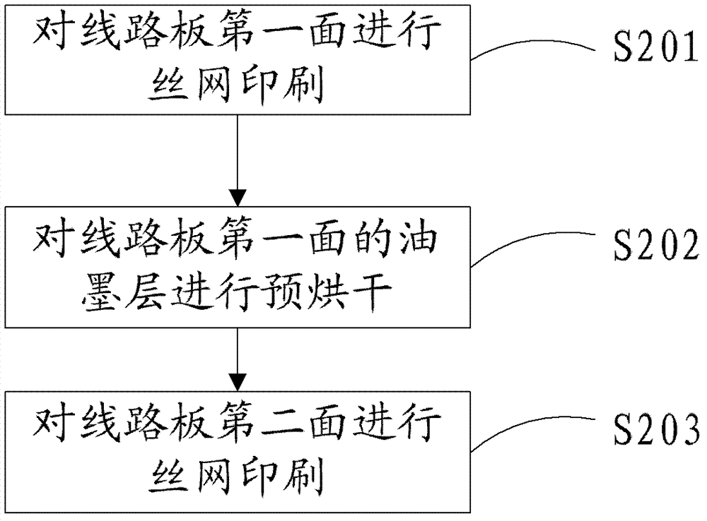
[0046] S20: scree...


PUM

PropertyMeasurementUnit
Thicknessaaaaaaaaaa

Abstract

The invention discloses a solder resisting method for a circuit board. The solder resisting method for the circuit board includes the following steps, a step 20 is that a first ink layer is printed in a silk-screen printing mode, more specifically, a silk screen with blocking points is utilized for printing the first ink layer, the blocking points cover holes in the circuit board, each blocking point is 0.13 to 0.17 millimeter longer than the diameter of each hole in the circuit board, and the thickness of the first ink layer is 35 micro meters to 40 micro meters; a step 30 is that a standing process is carried out on the circuit board; a step 40 is that a second ink layer is painted in an electrostatic spraying mode, more specifically, the electrostatic spraying technology is utilized for spraying the second ink layer on the circuit board, the second ink layer covers the first ink layer, and the thickness of the second ink layer is 40 micro meters to 50 micro meters; and a step 50 is that a solder resisting curing process is carried out, more specifically, the first ink layer and the second ink layer are exposed, developed and cured. The solder resisting method for the circuit board integrates the advantages of two solder resisting technologies, namely silk-screen printing and electrostatic spraying, the requirement that no solder resisting ink enters the holes of the circuit board is met, the technological processes are simple, and processing efficiency is high.

Description

technical field [0001] The invention relates to the field of printed circuit board processing, in particular to a circuit board solder resistance method. Background technique [0002] First, the relevant terms in the field of printed circuit board processing are explained: [0003] Solder resistance: Provide a permanent protective film for circuit boards with solder resistance, insulation, physical and chemical protection functions. This protective film can also be used as a carrier for text ink printing and make circuit boards have a beautiful appearance. [0004] Electrostatic spraying process: Using high-efficiency electrostatic characteristics and high-pressure spraying principle, the ink is charged with static electricity and attached to the surface of the circuit board, and the board after the ink is evenly sprayed is pre-baked to achieve the purpose of solder resistance. [0005] Nail bed process: In the solder resist process, copper nails of different specifications...

Claims


Application Information

Patent Timeline
IPC IPC(8): H05K3/28
Inventor 饶猛沙雷许瑛许克锋
Owner SHENNAN CIRCUITS
Why Eureka
Try Eureka