Press-in type high thermal conductive printed circuit board (PCB) and manufacture method thereof

A technology for a PCB board and a manufacturing method is applied in the field of press-in type high thermal conductivity PCB board and its manufacturing, which can solve the problems of looseness, falling off, and weak connection of copper blocks, and achieves the advantages of not easy to loose, realizing electrical connection, and shortening the process flow. Effect

Active Publication Date: 2013-05-08
NEW FOUNDER HLDG DEV LLC +1
View PDF7 Cites 27 Cited by
  • Summary
  • Abstract
  • Description
  • Claims
  • Application Information

AI Technical Summary

Problems solved by technology

[0011] The embodiment of the present invention provides a press-in high thermal conductivity PCB board and its manufacturing method, which is used to solve the problem that the connection between the pressed-in copper block and the PCB substrate is not firm in the prior art. When handling, it is easy to cause loosening or even falling off of the pressed copper block

Method used


Image

  • Press-in type high thermal conductive printed circuit board (PCB) and manufacture method thereof
  • Press-in type high thermal conductive printed circuit board (PCB) and manufacture method thereof
  • Press-in type high thermal conductive printed circuit board (PCB) and manufacture method thereof

Examples


Embodiment Construction

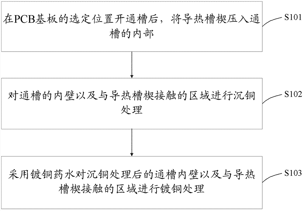
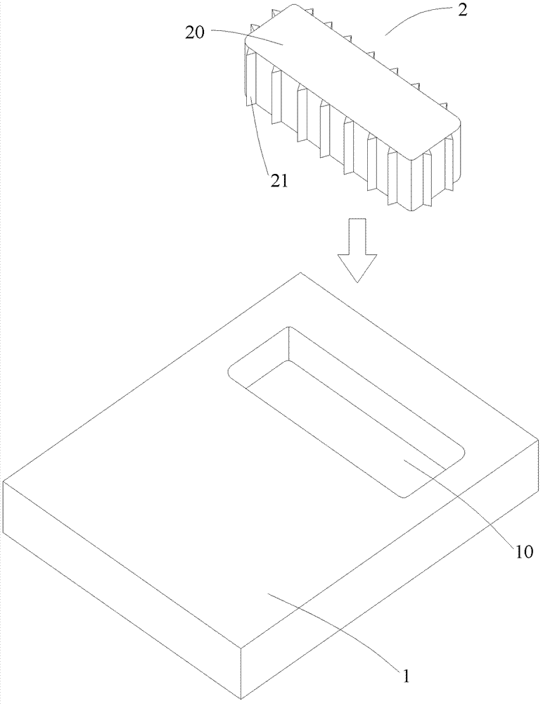
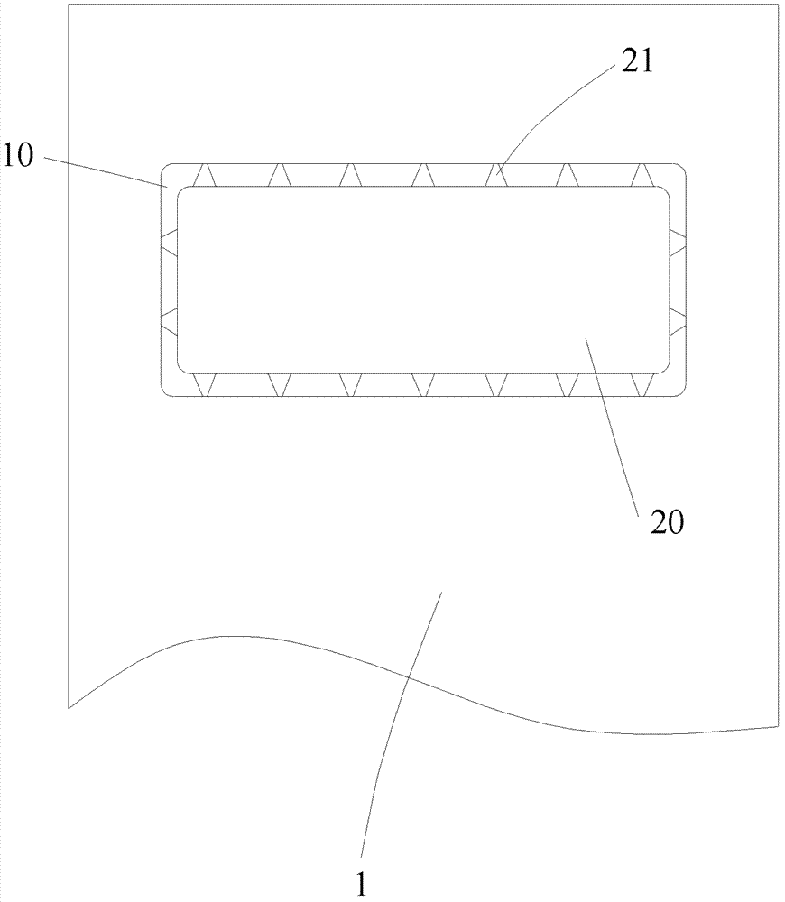
[0031] In the background technology, the process flow of making high thermal conductivity PCB board is long, and since the pressed-in copper block is rigidly connected to the groove wall of the through groove of the PCB substrate, the connection between the pressed-in copper block and the PCB substrate is not firm. , During copper sinking and copper plating, it is easy to cause the pressed copper block to loosen or even fall off. The embodiment of the present invention not only shortens the process flow of making high heat conduction PCB boards, but also makes the heat conduction The slot wedge is fixed in the through slot and is not easy to loose; and because the copper plating solution with high copper and low acid configuration is used to plate copper on the inner wall of the through slot after copper sinking treatment and the area in contact with the heat conduction slot wedge, the copper plated It can tightly wrap the contact point between the heat conduction wedge and th...


PUM


Abstract

The invention relates to the technical field of printed wiring board manufacture, in particular to a press-in type high thermal conductive printed circuit board (PCB) and manufacture method of the press-in type high thermal conductive PCB. The press-in type high thermal conductive PCB and the manufacture method of the press-in type high thermal conductive PCB are mainly used for solving the problems in the prior art that the connection between a press-in copper block and a PCB base plate is not firm, and looseness and even falling off of the press-in copper block is easy to happen in copper deposition and electroplating. The manufacture method of the press-in type high thermal conductive PCB comprises the steps: a through groove is formed in a chosen position of the PCB base board, a heat conductive slot wedge is pressed inside the through groove, copper deposition is conducted to the inner wall of the through groove and the contact area of the inner wall of the through groove and the heat conductive slot wedge, and copper plating is conducted to the inner wall of the through groove and the contact area of the inner wall of the through groove and the heat conductive slot wedge after copper deposition through copper plating liquid medicine. By means of the press-in type high thermal conductive PCB and the manufacture method of the press-in type high thermal conductive PCB, the technological process in high thermal conductive PCB manufacture is shortened, and the heat conductive slot wedge in a completed PCB is not easy to loosen.

Description

technical field [0001] The invention relates to the technical field of printed circuit board manufacturing, in particular to a press-in high thermal conductivity PCB board and a manufacturing method thereof. Background technique [0002] Printed Circuit Board (PCB) is an important electronic component. With the widespread use of high-frequency electronic signals, components such as chips on the PCB, especially high-power components, will generate a lot of heat when they work. If the heat generated by the components is not dissipated in time, it will damage the components. Cause a lot of damage, or even burn components. Therefore, how to effectively dissipate the high heat generated by the components on the PCB during operation at any time has become one of the key issues in PCB manufacturing. [0003] At present, the copper block with heat conduction function is pressed into the PCB substrate by pressing to form a high thermal conductivity PCB board. The heat generated by ...

Claims


Application Information

Patent Timeline
Patent Type & Authority Applications(China)
IPC IPC(8): H05K3/32
Inventor 黄翔陈正清
Owner NEW FOUNDER HLDG DEV LLC
Why Eureka
Try Eureka