Method for measuring thermal resistance of multi-layer heat-conducting material

A heat-conducting material and measurement method technology, applied in the field of testing, can solve the problems of not being able to find the problem quickly and conveniently, and not be able to analyze the thermal resistance composition of multi-layer heat-conducting materials, etc., and achieve the effect of high precision

Inactive Publication Date: 2013-05-15
BEIJING UNIV OF TECH
View PDF3 Cites 34 Cited by
  • Summary
  • Abstract
  • Description
  • Claims
  • Application Information

AI Technical Summary

Problems solved by technology

However, this method cannot analyze the composition of thermal resistance of different layers of materials inside the multilayer thermal conductive material, and cannot quickly and conveniently find the problem, that is, which layer of material thermal resistance is too large to have a major impact on the life of the device

Method used


Image

  • Method for measuring thermal resistance of multi-layer heat-conducting material
  • Method for measuring thermal resistance of multi-layer heat-conducting material
  • Method for measuring thermal resistance of multi-layer heat-conducting material

Examples


Embodiment Construction

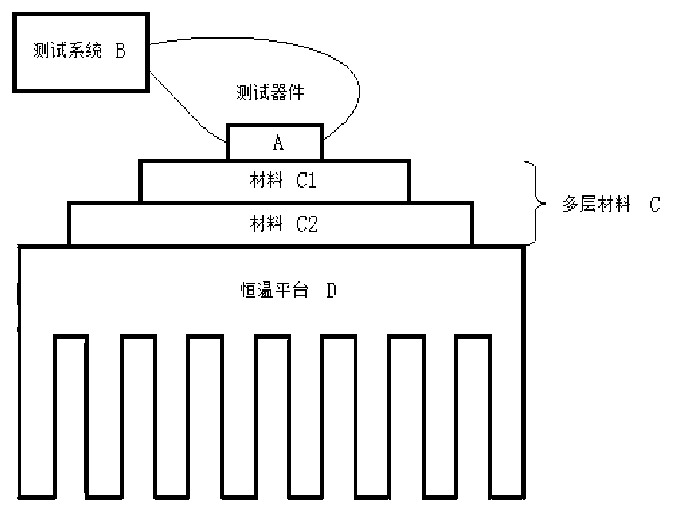
[0034] 1. The semiconductor device A is a power light-emitting diode; figure 1 As shown, from top to bottom, the semiconductor device A and the multi-layer heat-conducting material C are fixed on the constant temperature platform D in sequence;

[0035] Among them, the temperature coefficient of the PN junction and Schottky junction of the semiconductor device A is about -1~2mV / K, and the error of this value is not more than 7% between the absolute temperature of 275K and 475K;

[0036] The measurement system B includes: acquisition board B1, used to collect the voltage across the semiconductor device A; constant current source B2, used to provide the test current of the semiconductor device A; constant current source B3, used to provide the heating current of the semiconductor device A; computer B4 is used to control the opening of the acquisition board B1, and the constant current sources B2 and B3 provide heating current and test current on and off;

[0037] The multi-laye...


PUM


Abstract

The invention discloses a method for measuring the thermal resistance of a multi-layer heat-conducting material, which relates to the field of testing, and can be used for measuring the thermal resistance of each material layer in the multi-layer heat-conducting material. A semiconductor device in a testing system has a heat source function and a testing function. The method comprises the following steps of: fixing the semiconductor device on the upper surface of the multi-layer heat-conducting material, and fixing the lower surface of the multi-layer heat-conducting material on a constant temperature platform; and applying operating current to the semiconductor device for a period of time at any moment, removing the operating current after a steady state is achieved, and measuring a change curve of the junction temperature of the semiconductor device along with the time under the testing current. Because the thermal resistance, thermal capacity and heat transfer rate of each material layer in the multi-layer heat-conducting material are different, the thermal resistance and thermal capacity of each heat-conducting material layer are reflected through the measured change curve of the junction temperature of the semiconductor device along with the time; and according to a structure function method, the thermal resistance composition in each material layer in the multi-layer heat-conducting material is calculated. Moreover, the method belongs to non-destructive testing.

Description

Technical field: [0001] This technology relates to the field of testing technology. It is mainly used in the measurement and analysis of the thermal resistance of multi-layer heat-conducting materials. Background technique: [0002] Semiconductor devices will generate a lot of heat during operation, resulting in an increase in the temperature of the internal chip and shell of the semiconductor device. If the semiconductor device under working conditions is in an environment with poor heat dissipation channels, the device itself will accumulate a large amount of heat, which will lead to the degradation of various performance parameters of the semiconductor device and seriously affect the reliability and life of the semiconductor device. Manufacturing a good heat dissipation channel can remove the heat generated by the semiconductor device in time and ensure that the device is in a relatively stable temperature environment. Therefore, the analysis of the thermal resistance o...

Claims


Application Information

Patent Timeline
Patent Type & Authority Applications(China)
IPC IPC(8): G01N25/00
Inventor 郭春生万宁冯士维张燕峰石磊史冬
Owner BEIJING UNIV OF TECH
Why Eureka
Try Eureka