Structure of thin-layer thermal resistance test probe and test method

A technology for testing probes and thermal resistance, applied in the direction of material thermal development, material thermal conductivity, etc., can solve problems such as inapplicable fine structure thermal reliability analysis, inability to extract temperature information, incomplete thermal resistance structure, etc., reaching the scope of application wide, improve sensitivity and signal-to-noise ratio, and smooth the surface

Active Publication Date: 2020-06-16
BEIJING UNIV OF TECH
View PDF20 Cites 2 Cited by
  • Summary
  • Abstract
  • Description
  • Claims
  • Application Information

AI Technical Summary

Problems solved by technology

However, due to the different electrical states of the semiconductor device between the heating stage and the measurement stage, there is often a microsecond-level switching delay time
This delay makes it impossible to extract the temperature information during this period, and the resulting thermal resistance structure is incomplete
Therefore, this switch-type measurement method is no longer suitable for thermal reliability analysis of fine structures.
However, optical measurement often requires huge and expensive optical equipment, and due to the limitations of materials and measurement principles, the measured samples often need to be specially prepared.

Method used


Image

  • Structure of thin-layer thermal resistance test probe and test method
  • Structure of thin-layer thermal resistance test probe and test method

Examples


Embodiment Construction

[0020] The present invention will be further described below in conjunction with accompanying drawing and specific embodiment:

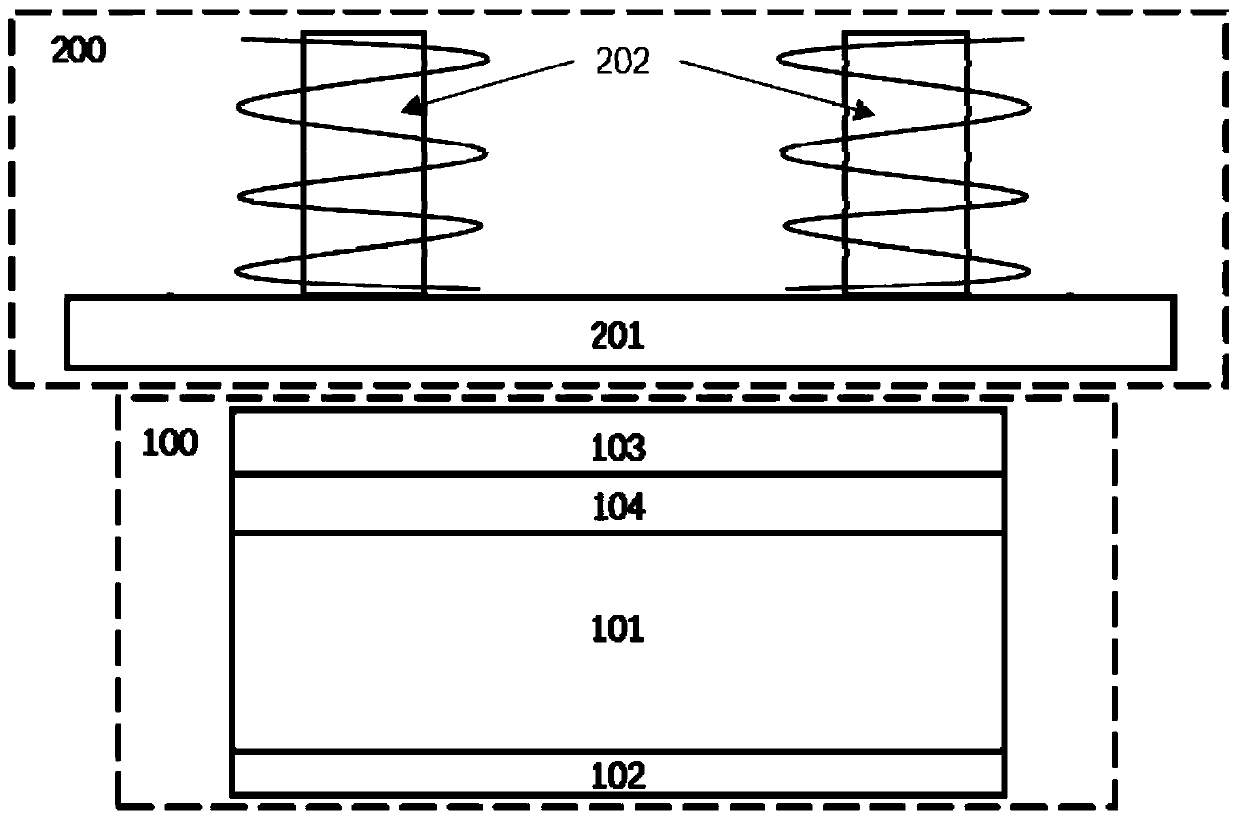
[0021] like figure 1 A schematic diagram of the structure of a thin-layer thermal resistance test probe is shown, including, 100: probe chip; 101: substrate structure; 102: measurement source; 103: heating source; 104: heat spreading layer; 200: packaging structure; 201 : substrate; 202: spring support structure;

[0022] The probe chip 100 is made of a measurement source 102, a heating source 103 and a heat soaking layer 104 on a semiconductor substrate material 101 through semiconductor processes such as photolithography, ion implantation and photolithography;

[0023] The measurement source 102 consists of multiple diodes connected in series and in parallel to form a temperature probe, with a total chip area of ​​about 1.5mm×1.5mm. The change of the forward junction voltage drop of each diode with temperature is about 2mV / °C. When 10 diodes are ...


PUM


Abstract

The invention discloses a structure of a thin-layer thermal resistance test probe and a test method, and belongs to the technical field of electrical and thermal tests of semiconductor materials and devices. The structure comprises a probe chip and a packaging structure, wherein the probe chip comprises a temperature probe formed by connecting a plurality of diodes in series and in parallel, a micro heater formed by doping polycrystalline silicon patterns, a lead electrode and a semiconductor substrate material; the packaging structure comprises a substrate used for fixing the probe chip and the extraction electrode, and a spring supporting structure used for moving the probe chip and applying pressure. The invention designs a thin-layer thermal resistance test probe structure composed ofa Si-based temperature measurement probe chip adopting a double-sided process. By adopting the structural design that the heating source and the measuring source are separated, the heating state and the measuring state can be carried out at the same time, switching delay does not exist, and non-switching type thermal resistance measurement can be carried out on a semiconductor chip and a thin-layer material.

Description

Technical field: [0001] The invention discloses a structure and a testing method of a thin-layer thermal resistance testing probe, belonging to the technical field of electrical and thermal measurement of semiconductor materials and devices. The structure includes: a chip structure and a packaging structure. Background technique: [0002] With the development of thermal resistance testing towards the microscopic field and refinement, the measurement of device-level thermal resistance can no longer meet the reliability research of some devices. The interface thermal resistance of different materials during the growth process and the body heat of the material itself Fine structure thermal resistance such as resistance has increasingly become the focus of attention. Compared with the bulk material, it has good compactness and integrity. The interface of heterogeneous materials is often subject to phenomena such as increased material defects and phonon mismatch due to lattice m...

Claims


Application Information

Patent Timeline
Patent Type & Authority Applications(China)
IPC IPC(8): G01N25/20G01N25/18
CPCG01N25/20G01N25/18
Inventor 冯士维李轩郑翔何鑫白昆潘世杰
Owner BEIJING UNIV OF TECH
Why Eureka
Try Eureka