Conducting film and preparation method thereof and touch screen comprising the same

A technology of conductive film and conductive layer, applied in the field of electronics, can solve the problems of large thickness of touch screen, unfavorable development of thin and light electronic products, etc., achieve the effect of small thickness, improve processing efficiency, and simplify process flow

Active Publication Date: 2013-05-15
江西卓讯微电子有限公司
View PDF4 Cites 72 Cited by
  • Summary
  • Abstract
  • Description
  • Claims
  • Application Information

AI Technical Summary

Problems solved by technology

Therefore, the traditional conductive film bonding will make the touch screen have a large thickness, which is not conducive to the development of electronic products in the direction of thinner and lighter

Method used


Image

  • Conducting film and preparation method thereof and touch screen comprising the same
  • Conducting film and preparation method thereof and touch screen comprising the same
  • Conducting film and preparation method thereof and touch screen comprising the same

Examples


Embodiment Construction

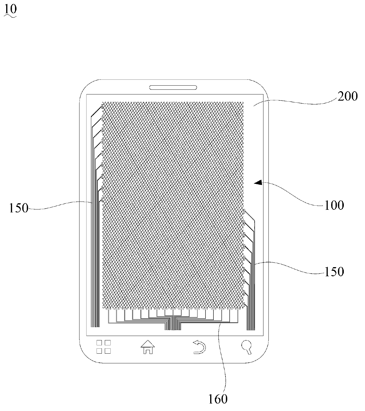
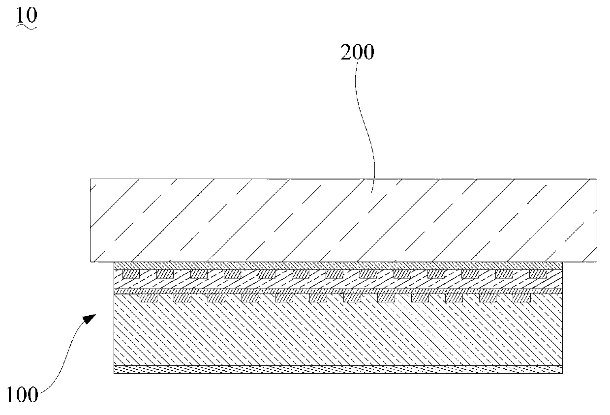
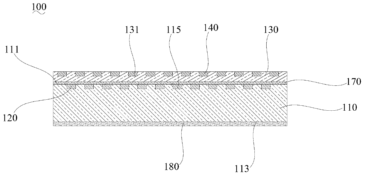
[0053] In order to facilitate the understanding of the present invention, the present invention will be described more fully below with reference to the associated drawings. Preferred embodiments of the invention are shown in the accompanying drawings. However, the present invention can be embodied in many different forms and is not limited to the embodiments described herein. On the contrary, these embodiments are provided to make the understanding of the disclosure of the present invention more thorough and comprehensive.

[0054] It should be noted that when an element is referred to as being “fixed” to another element, it can be directly on the other element or there can also be an intervening element. When an element is referred to as being "connected to" another element, it can be directly connected to the other element or intervening elements may also be present.

[0055] Unless otherwise defined, all technical and scientific terms used herein have the same meaning as...


PUM

PropertyMeasurementUnit
widthaaaaaaaaaa
widthaaaaaaaaaa
thicknessaaaaaaaaaa

Abstract

The invention discloses a conducting film which comprises a base sheet, a first conducting layer, a substrate layer and a second conducting layer, wherein the base sheet comprises a first surface and a second surface which is arranged opposite to the first surface, and the first conducting layer is embedded in the base sheet. The substrate layer is attached to the first surface of the base sheet and is formed by curing a jelly like substance coated on the first surface. The second conducting layer is embedded in the substrate layer and is insulated from the first conducting layer by the substrate layer. Due to the fact that capacitance can form between the first conducting layer and the second conducting layer, when the conducting film is used for manufacturing a touch screen, two conducting films do not need to be combined together in a bonding mode, and all that is needed is to attach the conducting film to a glass panel. In addition, the substrate layer is formed by curing the jelly like substance coated on the base sheet, the thickness is far smaller than that of the base sheet, and therefore the touch screen made of the conducting film has a quite small thickness. Moreover, the invention further provides a preparation method of the conducting film and the touch screen comprising the conducting film.

Description

technical field [0001] The invention relates to electronic technology, in particular to a conductive film, a preparation method thereof and a touch screen containing the conductive film. Background technique [0002] Conductive film is a thin film with good conductivity and flexibility. At present, it is mainly used in touch screen and other fields, and has a very broad market space. A conventional conductive film includes a substrate and a conductive layer formed on the substrate. The conductive layer is formed on the substrate by processes such as coating and spraying. When this kind of conductive film is used in practical applications, it is usually necessary to bond two pieces of conductive film together with an adhesive to make it suitable for special purposes, such as electromagnetic screen film, touch sensitive film, etc. [0003] Taking the conductive film used in the touch screen of a mobile phone as an example, two conductive films are glued together by opticall...

Claims


Application Information

Patent Timeline
Patent Type & Authority Applications(China)
IPC IPC(8): H01B5/14H01B13/00G06F3/044
CPCG06F3/044H01B5/14G06F3/0445G06F3/0446G06F3/041H01B13/00
Inventor 高育龙崔铮孙超
Owner 江西卓讯微电子有限公司
Why Eureka
Try Eureka