

Method for manufacturing passivation layer on pixel electrode, liquid crystal display and manufacturing method thereof
A technology of liquid crystal display and manufacturing method, which is applied to instruments, circuits, electrical components, etc., can solve problems such as inability to display and abnormal display of TFT products, and achieve the effects of improving yield, ensuring good electrical contact, and reducing losses
- Summary
- Abstract
- Description
- Claims
- Application Information
AI Technical Summary
Problems solved by technology
Method used
Image

Examples
Embodiment 1
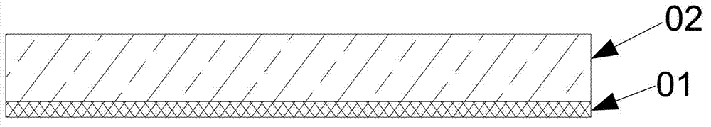
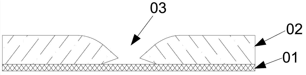
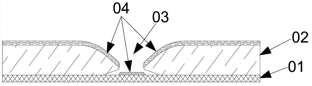
[0038] Such as Figure 4 As shown, the method for manufacturing the passivation layer on the pixel electrode provided by the embodiment of the present invention includes: forming a passivation layer 12 with a first thickness on the surface of the pixel electrode 11 under the first power and using the process gas of the first flow rate ; Under the second power, the process gas of the second flow rate is used to form the passivation layer 13 of the second thickness on the surface of the passivation layer 12 of the first thickness; wherein, the first power is less than the second power; The first flow rate is smaller than the second flow rate; the first thickness is smaller than the second thickness.
[0039] In one embodiment of the present invention, the passivation layer is a silicon nitride layer, and the process gas in its fabrication process includes SiH 4and NH 3 . In the following embodiments of the present invention, the passivation layer is a silicon nitride layer as...
PUM
 Abstract
Description
Claims
Application Information