Light field imaging device and image processing device

一种光场摄像、摄像面的技术,应用在三维摄像技术领域,能够解决无法同时获得高分辨率图像和深度信息等问题

Active Publication Date: 2013-05-22
PANASONIC INTPROP MANAGEMENT CO LTD
View PDF13 Cites 15 Cited by
  • Summary
  • Abstract
  • Description
  • Claims
  • Application Information

AI Technical Summary

Problems solved by technology

However, there is a problem with this technology that a mechanism for changing the focal length of the microlens and a mechanism for controlling it are required, and high-resolution images and depth information cannot be obtained at the same time

Method used


Image

  • Light field imaging device and image processing device
  • Light field imaging device and image processing device
  • Light field imaging device and image processing device

Examples


Embodiment approach 1

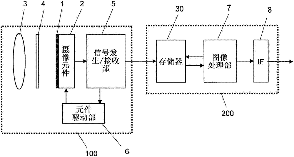
[0055] First, an imaging device according to a first embodiment of the present invention will be described. figure 1 It is a block diagram showing a schematic configuration of a light field imaging device (hereinafter, simply referred to as "imaging device") according to this embodiment. The imaging device of this embodiment is a digital electronic camera, and includes an imaging unit 100 and a signal processing unit 200 that generates a signal (image signal) representing an image based on a signal generated by the imaging unit 100 .

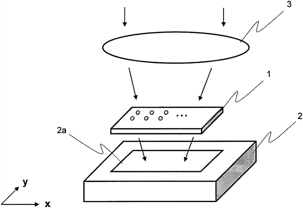
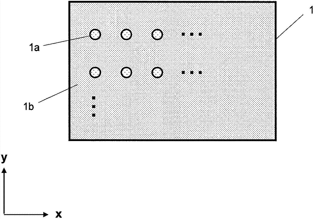
[0056] The imaging section 100 includes the following: a color solid-state imaging element 2 (hereinafter simply referred to as "imaging element") having a plurality of photosensitive elements arranged on an imaging surface; Light-transmitting plate 1 (light-transmitting part) of two kinds of light-transmitting areas different from each other; circular optical lens 3 (imaging part) for forming an image on imaging surface 2a of imaging element 2;...

Embodiment approach 2

[0121] Next, a second embodiment of the present invention will be described. In this embodiment, the primary color configurations of the optical lens 3 and the imaging element 2 are different from those of the first embodiment described above, but are the same as those of the first embodiment. Hereinafter, the description will focus on points different from Embodiment 1, and the description of the same matters will be omitted.

[0122] Figure 7 It is a figure which shows the imaging state of the optical lens 3 of this embodiment. In the present embodiment, the optical lens 3 has different focal lengths between the peripheral portion 3a and the central portion 3b. The focal length is relatively short in the lens peripheral portion 3a, and the focal length is relatively long in the lens central portion 3b. Based on this characteristic, the subject is brought into focus on the light-transmitting plate 1 with respect to the lens peripheral portion 3a, and the subject is brough...

Embodiment approach 3

[0129] Next, a third embodiment of the present invention will be described. In this embodiment, on the light-incident side surface (front face) of the optical lens 3 of Embodiment 2, two kinds of light-transmitting lenses having the same spectral transmittance characteristics as the two kinds of light-transmitting regions of the light-transmitting plate 1 are arranged. member. Specifically, as Figure 9 As shown, in front of the peripheral portion 3a of the lens 3, a light-transmitting member 1aa having the same spectral transmittance characteristics as the light-transmitting region 1a of the light-transmitting plate 1 is disposed, and in front of the central portion 3b of the lens 3, a light-transmitting member 1aa is disposed. A light-transmitting member 1bb having the same spectral transmittance characteristic as that of the light-transmitting region 1b of the light-transmitting plate 1 was obtained. Other configurations and processes are the same as those in Embodiment 2...


PUM


Abstract

The invention provides an imaging device. This imaging device is provided with: an imaging element (2) containing a first type of pixel and a second type of pixel having mutually different spectral transmission factor characteristics; a light transmission section (1) disposed in a manner so as to face the imaging surface of the imaging element (2); and an image formation unit (3) having at least a first image formation region having a first focal distance and a second image formation region having a second focal distance that is longer than the first focal distance. The light transmission section (1) has a first light transmission region (1a) configured from a plurality of mutually separated partial regions, and a second light transmission region (1b) having different spectral transmission factor characteristics from the first light transmission region (1a). The distance between the light transmission section (1) and the image formation unit (3) is equivalent to the first focal distance (f1) and the distance between the imaging surface of the imaging element (2) and the image formation unit (3) is equivalent to the second focal distance (f2).

Description

technical field [0001] The present application relates to monocular three-dimensional imaging technology that generates multi-viewpoint images using one optical system and one imaging element. Background technique [0002] In recent years, digital still cameras and digital video cameras using solid-state imaging devices such as CCDs and CMOSs ​​(hereinafter referred to as "imaging devices") have become eye-opening in terms of higher functionality and higher performance. In particular, the miniaturization of the pixel structure of an imaging element is progressing along with the advancement of semiconductor manufacturing technology. As a result, high integration of pixels and drive circuits of the imaging element can be achieved. As a result, the number of pixels in an imaging element has increased significantly from around 1 million pixels to more than 10 million pixels in just a few years. In addition, the quality of captured images has also been dramatically improved. O...

Claims


Application Information

Patent Timeline
Patent Type & Authority Applications(China)
IPC IPC(8): G03B35/08G02B3/00G03B11/00H04N5/225H04N9/07H04N13/271
CPCG02B3/00G06T11/006G06T17/00G06T7/0065H04N9/07H04N13/0217H04N13/02G03C9/00G02B27/0075G03B11/00G06T2207/10052H04N13/0271H04N9/045G03B35/10H04N5/225G03B35/08G06T7/557H04N13/20H04N13/218H04N13/271H04N23/957H04N23/00H04N25/134
Inventor 平本政夫石井育规
Owner PANASONIC INTPROP MANAGEMENT CO LTD
Why Eureka
Try Eureka