Forming method of metal oxide semiconductor (MOS) device and MOS device formed through method

A technology of MOS devices and epitaxy, which is applied in semiconductor devices, semiconductor/solid-state device manufacturing, electrical components, etc., can solve problems such as leakage, and achieve the effect of less leakage.

Active Publication Date: 2015-07-08
SEMICON MFG INT (SHANGHAI) CORP
View PDF5 Cites 0 Cited by
  • Summary
  • Abstract
  • Description
  • Claims
  • Application Information

AI Technical Summary

Problems solved by technology

[0006] The problem to be solved by the present invention is to propose a new method for forming MOS devices, which solves the problem that the existing MOS devices have defects in the source and drain during the production process, and leakage occurs during use.

Method used


Image

  • Forming method of metal oxide semiconductor (MOS) device and MOS device formed through method
  • Forming method of metal oxide semiconductor (MOS) device and MOS device formed through method
  • Forming method of metal oxide semiconductor (MOS) device and MOS device formed through method

Examples


Embodiment Construction

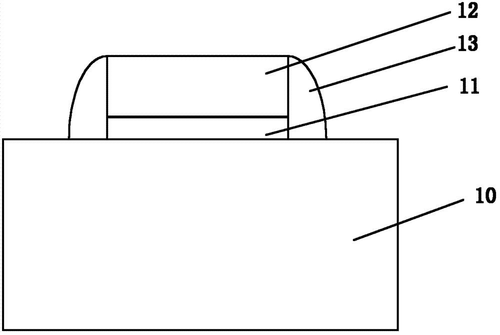
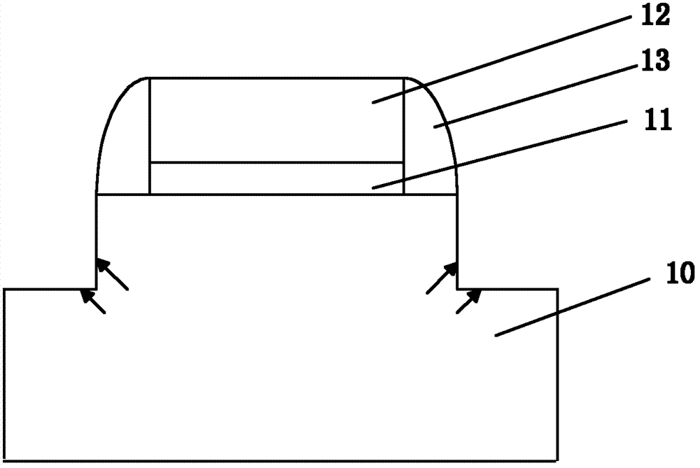
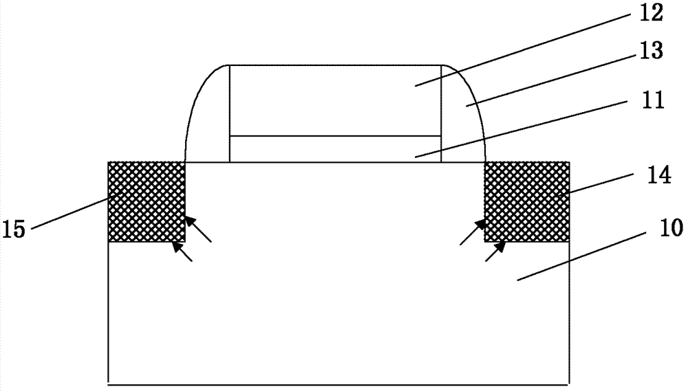
[0045] When forming the silicon-germanium source and drain in the existing MOS structure, the semiconductor substrate is first etched by a self-aligned method, which may cause large defects in the semiconductor substrate. The MOS structure with this defect will leak electricity from the source region and the drain region to the substrate during use. To solve this problem, the inventor of the present invention proposes to first use an epitaxial method to form an epitaxial layer located in the channel region, the epitaxial layer is exactly the same material and lattice structure as the semiconductor substrate, and then to etch the epitaxial layer using an isotropic etching method. The epitaxial layer avoids the use of the self-aligned method used in the prior art to etch the semiconductor substrate, thus reducing the damage formed in the semiconductor substrate at the intersection of the source region and the drain region with the semiconductor substrate. For the purpose of reduc...


PUM


Abstract

The invention provides a forming method of a metal oxide semiconductor (MOS) device. The forming method comprises first providing a semiconductor substrate at least comprising three regions, enabling a first region to be used for forming a gate region, enabling a second region and a third region which are adjacent to the first region to be respectively used for forming a source region and a drain region; utilizing an epitaxial method to the semiconductor substrate of the first region to extend outwards to grow an epitaxial layer; then utilizing an isotropic etching method to etch the epitaxial layer to form a channel region; then utilizing the epitaxial method to grow silicon-germanium in the second region and the third region, and respectively forming a silicon-germanium source region structure and a drain region structure; and then doping the silicon-germanium source region structure and the drain region structure. The invention further provides the MOS device formed by utilizing the method. Due to the technical scheme, damage to a silicon substrate caused by etching of the source region and the drain region in a conventional method is avoided, the goal of reducing defects is achieved, and electric leakage of the formed MOS device in the using process cannot occur easily.

Description

Technical field [0001] The present invention relates to the field of semiconductor manufacturing, in particular to a method for forming a MOS device and a MOS device formed by the above method. Background technique [0002] MOS devices are one of the basic elements in integrated circuits. In recent years, the use of silicon-germanium as the source and drain to improve the performance of MOS devices has appeared in the semiconductor industry. It is known that when uniaxial compressive strain is directly applied from the silicon-germanium source and drain regions to the channel region of the transistor, the performance of the PMOS transistor can be improved. When uniaxial tensile strain is applied to the channel region, the performance of the NMOS transistor can be improved. [0003] Figure 1 to Figure 3 Shown are schematic diagrams of various structures formed in the manufacturing steps of a MOS device using silicon-germanium as the source and drain in the prior art. First, refer...

Claims


Application Information

Patent Timeline
Patent Type & Authority Patents(China)
IPC IPC(8): H01L21/336H01L29/78
Inventor 刘金华
Owner SEMICON MFG INT (SHANGHAI) CORP
Why Eureka
Try Eureka