A method for forming a shallow trench isolation structure

A technology of isolation structure and shallow trench, which is applied in electrical components, semiconductor/solid-state device manufacturing, circuits, etc., can solve the problem of poor isolation performance of shallow trench isolation structures, leakage of semiconductor devices, and influence on the stability of semiconductor devices, etc. problems, to achieve the effect of eliminating Q-time effect, improving the uniformity of film thickness, and not easy to leak

Active Publication Date: 2016-06-29
SHANGHAI HUALI MICROELECTRONICS CORP
View PDF5 Cites 0 Cited by
  • Summary
  • Abstract
  • Description
  • Claims
  • Application Information

AI Technical Summary

Problems solved by technology

However, compared with the traditional high-density plasma (HDPCVD) process, although the filling capacity of the SACVD process has been greatly improved, but at the same time when this process is applied, a new integration problem arises: in the middle of the trench oxide, a a vulnerable surface (such as figure 1 As shown by the dotted circle in the middle), this fragile surface is very susceptible to erosion by the subsequent wet process, which makes it difficult to control the uniformity of the subsequent process, resulting in poor isolation performance of the shallow trench isolation structure, including the shallow trench isolation structure. Semiconductor devices are prone to leakage, which seriously affects the stability of semiconductor devices containing shallow trench isolation structures

Method used


Image

  • A method for forming a shallow trench isolation structure
  • A method for forming a shallow trench isolation structure
  • A method for forming a shallow trench isolation structure

Examples


Embodiment Construction

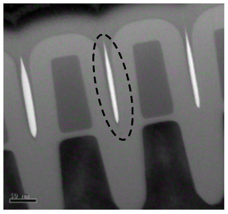
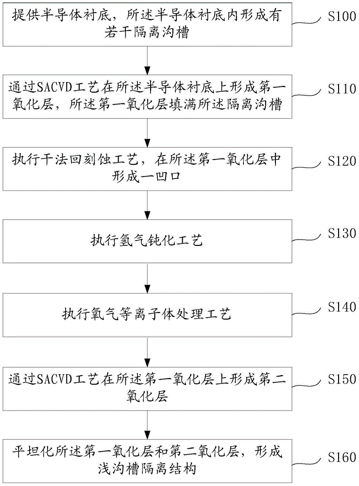
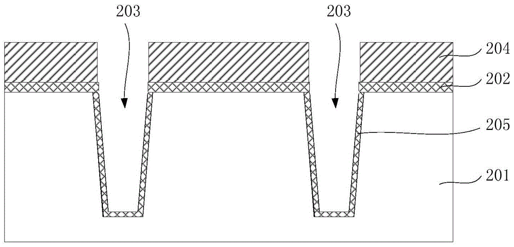
[0030] As mentioned in the background, with the continuous reduction of the feature size of semiconductor devices, the size of the shallow trench isolation structure used for device isolation is also reduced, and the aspect ratio of the isolation trench used to form the shallow trench isolation structure becomes smaller. Large, when the oxide layer is filled and formed in the isolation trench by the SACVD process, a fragile surface is likely to appear, resulting in poor isolation performance of the shallow trench isolation structure, and semiconductor devices including the shallow trench isolation structure are prone to leakage and poor stability. For this reason, after the first oxide layer is formed by the SACVD process in the present invention, the dry etching process is performed to eliminate the fragile surface, and then the second oxide layer is formed by the SACVD process, and then the planarization process is performed, and the shallow trench thus formed The isolation e...


PUM


Abstract

The invention provides a method for forming a shallow trench isolation structure. After a first oxidation layer is formed through the SACVD technology, the dry etching technology is executed to eliminate a fragile face of the first oxidation layer, and then a second oxidation layer is formed through the SACVD technology. The shallow trench isolation structure formed with the method is good in isolation effect, and a semiconductor device comprising the shallow trench isolation structure is good in stability and not prone to electric leakage and breakdown. Besides, the hydrogen passivation technology is added, unsaturated bonds on the surface of a film can be eliminated with the hydrogen passivation technology, and thus the deposition rate of the subsequent technology is stable, and finally the thickness uniformity of the film is improved. Furthermore, the oxygen plasma processing technology is adopted, hydrogen bonds on the surface and the surface layer of the structure are effectively removed through O2 plasma to eliminate the Q-time effect of the deposition rate of the subsequent manufacturing process, and thus the structure is more stable before the deposition of the subsequent manufacturing process.

Description

technical field [0001] The invention relates to the technical field of integrated circuit manufacturing, in particular to a method for forming a shallow trench isolation structure. Background technique [0002] As semiconductor technology enters the deep sub-micron era, components below 0.18 microns (such as between the active regions of CMOS integrated circuits) are mostly fabricated using shallow trench isolation (STI) for lateral isolation. With the continuous reduction of the feature size of semiconductor devices, the size of the shallow trench isolation structure used for device isolation is also reduced, and correspondingly, the aspect ratio of the isolation trench used to form the shallow trench isolation structure is increased. [0003] In the existing advanced manufacturing process, starting from the 45nm technology node, its shallow trench isolation process has begun to use the sub-atmospheric pressure chemical vapor deposition (SACVD) process to fill the trench ox...

Claims


Application Information

Patent Timeline
Patent Type & Authority Patents(China)
IPC IPC(8): H01L21/762
CPCH01L21/76224
Inventor 郑春生张文广
Owner SHANGHAI HUALI MICROELECTRONICS CORP
Why Eureka
Try Eureka