Organic light-emitting diodes (LEDs) and organic LED displayer composed of the same

A technology of light-emitting diodes and displays, applied in the manufacture of electric solid-state devices, semiconductor devices, semiconductor/solid-state devices, etc., which can solve problems such as difficult alignment, high cost, and difficult fabrication of metal masks 17, and achieve the effect of avoiding voltage drop

Active Publication Date: 2013-06-05
INNOCOM TECH SHENZHEN +1
View PDF4 Cites 28 Cited by
  • Summary
  • Abstract
  • Description
  • Claims
  • Application Information

AI Technical Summary

Problems solved by technology

However, in order to prevent the organic layer from covering the position of the exposed area 16 of the auxiliary electrode, a precise metal mask 17 ne

Method used


Image

  • Organic light-emitting diodes (LEDs) and organic LED displayer composed of the same
  • Organic light-emitting diodes (LEDs) and organic LED displayer composed of the same
  • Organic light-emitting diodes (LEDs) and organic LED displayer composed of the same

Examples


Embodiment Construction

[0062] In order to make the above-mentioned and other objects, features, and advantages of the present invention more comprehensible, the preferred embodiments are listed below, together with the accompanying drawings, and are described in detail as follows:

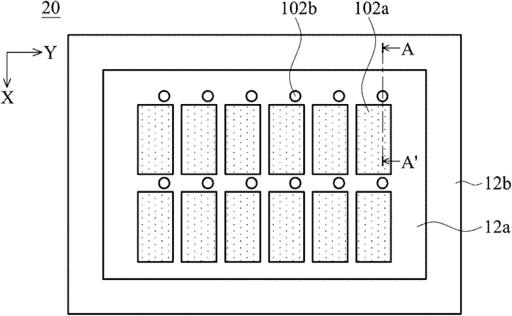
[0063] figure 2 It is a top view of the top emission (top emission) organic light emitting diode 20 of the present invention, Figure 3A , Figure 3B , Figure 3C to Figure 3D for a series of figure 2 The cross-sectional view of line AA' in the middle shows the fabrication method of the top emission (top emission) organic light emitting diode of the present invention. First, see Figure 3A , providing a substrate 101 . In the passive array organic light emitting diode display, the material of the substrate 101 is a common glass substrate, and may also be a plastic substrate in another embodiment. In an active matrix organic light emitting diode display, the substrate 101 is a thin film transistor (TFT) substrate,...


PUM


Abstract

The invention provides organic light-emitting diodes (LEDs) and an organic LED displayer composed of the same. Each organic LED comprises a substrate which comprises a pixel electrode area and an auxiliary electrode area, and an insulating layer formed between the pixel electrode area and the auxiliary electrode area, wherein the pixel electrode area comprises a first electrode formed on the substrate, an organic layer formed on the first electrode and a second electrode formed on the organic layer, and the auxiliary electrode layer comprises an auxiliary electrode formed on the substrate and a shielding structure formed on the auxiliary electrode or on the insulating layer. The shielding structure shields partial auxiliary electrode, and the second electrode is in electric connection with the auxiliary electrode.

Description

technical field [0001] The present invention relates to an organic light emitting diode, and in particular to an organic light emitting diode which avoids voltage drop and an organic light emitting diode display composed of the same. Background technique [0002] Organic light-emitting diodes (organic light-emitting diodes) are widely used in flat-panel displays due to their advantages of high brightness, lightness, thinness, no need for backlight sources, and low power consumption. [0003] See Figure 1A , which shows a top view of an existing organic light emitting diode 10, which includes a display area 12a and a peripheral area 12b located on the periphery of the display area 12a, and an auxiliary electrode contact hole (contact hole) 14 is located in the peripheral area 12b for connecting with the display area The upper electrode (not shown in the figure) of 12a is electrically connected. The power is input from the auxiliary electrode via hole 14 in the peripheral ar...

Claims


Application Information

Patent Timeline
IPC IPC(8): H01L51/52H01L27/32
CPCH10K59/1315H10K59/1795H10K50/824
Inventor 吴昶庆蔡旻翰黄浩榕
Owner INNOCOM TECH SHENZHEN
Why Eureka
Try Eureka