Infrared phase locking and imaging method and device for surface and subsurface defect detection of optimal element
A technology for subsurface defects and optical components, which is applied in the direction of optical testing defects/defects, etc., can solve the problems of surface and subsurface absorption defects of transparent optical components, weak absorption defects cannot be effectively identified, and low resolution, so as to improve detection Signal-to-noise ratio, high speed, and the effect of improving detection sensitivity
- Summary
- Abstract
- Description
- Claims
- Application Information
AI Technical Summary
Problems solved by technology
Method used
Image

Examples
Embodiment Construction
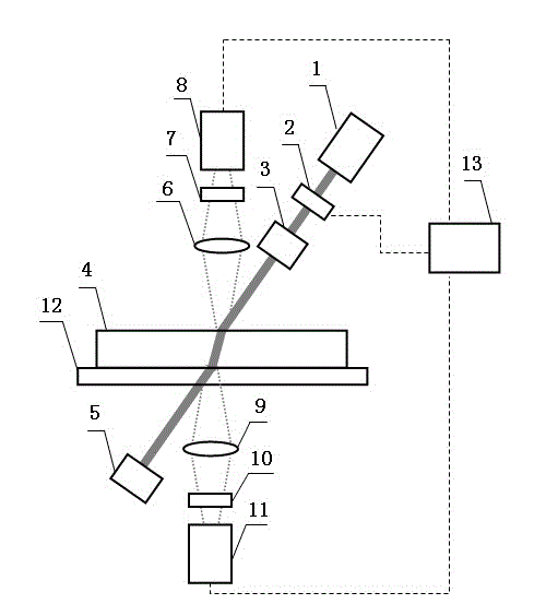
[0024] See figure 1 , an infrared phase-locked imaging device for detecting surface and subsurface defects of an optical element, including a pumping light source 1 arranged relative to the front surface of the optical element 4, and a pump sequentially arranged between the emitting end of the pumping light source 1 and the front surface of the optical element 4 The pump beam modulation device 2 and the pump beam shaping processing device 3, the pump light absorbing device 5 arranged on the rear surface of the optical element 4, and the first infrared imaging device 6 arranged on the front surface of the optical element 4 are sequentially arranged on the first infrared The first infrared filtering device 7 and the first infrared detector array 8 at the rear end of the imaging device 7, the second infrared imaging device 9 arranged on the rear surface of the optical element 1, and the second infrared filtering device arranged at the rear end of the second infrared imaging device...
PUM
 Abstract
Description
Claims
Application Information
 - R&D
- Intellectual Property
- Life Sciences
- Materials
- Tech Scout
- Unparalleled Data Quality
- Higher Quality Content
- 60% Fewer Hallucinations
Browse by: Latest US Patents, China's latest patents, Technical Efficacy Thesaurus, Application Domain, Technology Topic, Popular Technical Reports.
© 2025 PatSnap. All rights reserved.Legal|Privacy policy|Modern Slavery Act Transparency Statement|Sitemap|About US| Contact US: help@patsnap.com