
Infrared phase locking and imaging method and device for surface and subsurface defect detection of optimal element

A technology for subsurface defects and optical components, applied in the direction of optical testing flaws/defects, etc., can solve the problems of low sensitivity, low resolution, surface and subsurface absorption defects of transparent optical components, etc., to suppress useless noise and improve detection. Signal-to-noise ratio, the effect of improving detection sensitivity

Active Publication Date: 2015-06-24
合肥利弗莫尔仪器科技有限公司
View PDF13 Cites 0 Cited by
  • Summary
  • Abstract
  • Description
  • Claims
  • Application Information

AI Technical Summary

Problems solved by technology

The advantage of this method is that the imaging speed is fast; the disadvantage is that the imaging resolution depends on the infrared detector array and its related infrared imaging system. effective identification
[0005] To sum up, there is currently no good detection method that can be used to directly detect the surface and subsurface absorption defects of large-aperture optical components, especially the surface and subsurface absorption defects of transparent optical components with relatively weak absorption.

Method used


Image

  • Infrared phase locking and imaging method and device for surface and subsurface defect detection of optimal element

Examples


Embodiment Construction

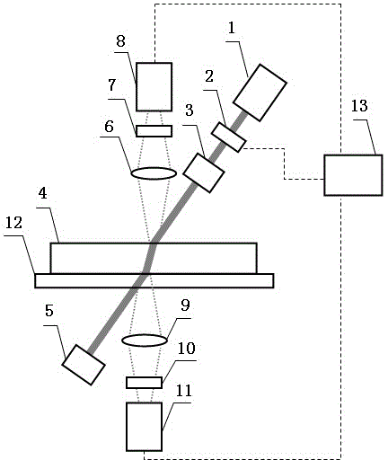
[0023] See figure 1 , an infrared phase-locked imaging device for detecting surface and subsurface defects of an optical element, including a pumping light source 1 arranged relative to the front surface of the optical element 4, and a pump sequentially arranged between the emitting end of the pumping light source 1 and the front surface of the optical element 4 The pump beam modulation device 2 and the pump beam shaping processing device 3, the pump light absorbing device 5 arranged on the rear surface of the optical element 4, and the first infrared imaging device 6 arranged on the front surface of the optical element 4 are sequentially arranged on the first infrared The first infrared filtering device 7 and the first infrared detector array 8 at the rear end of the imaging device 7, the second infrared imaging device 9 arranged on the rear surface of the optical element 1, and the second infrared filtering device arranged at the rear end of the second infrared imaging device...


PUM


Abstract

The invention discloses infrared phase locking and imaging method and device for surface and subsurface defect detection of an optimal element. The method and the device provided by the invention combine an infrared imaging technology with a phase locking amplification and detection technology; high-resolution image information related to the defect of a sample can be obtained by using a modulated pump laser excitation sample to generate periodic infrared radiation, using an infrared detection array to detect the generated infrared radiation, and carrying out phase locking amplification and detection on signals of the infrared detection array; and meanwhile, the influence of infrared signals inside a sample body on a detection result is eliminated by using the physical property that the penetration depth of the excited infrared radiation on some optical materials within a selected waveband is very limited, so that the imaging detection is only carried out on absorption defect distribution of the surface and subsurface of the sample. The method and the device are applicable to the detection and the imaging of the surface and subsurface absorption defect of the optical element, and are particularly suitable for the detection and the imaging of the surface and subsurface absorption defect of the common large-caliber optical element in an outsize high-power laser system.

Description

technical field [0001] The invention relates to the field of detection methods for surface and subsurface defects of optical elements, in particular to an infrared lock-in imaging method and device for detecting surface and subsurface defects of optical elements. Background technique [0002] In high-power or high-energy intense laser systems and their applications, the laser damage threshold of optical components is often a key factor restricting the operating level of related systems. The laser damage threshold of these optical components is often well below the intrinsic damage threshold of the material used to make the component. Taking the large-aperture fused silica element used in the laser inertial confinement fusion system as an example, its damage threshold in the 355nm ultraviolet laser band is much lower than the intrinsic threshold of the pure quartz material used to make the element, which restricts related systems. One of the key factors in design and develop...

Claims


Application Information

Patent Timeline
Patent Type & Authority Patents(China)
IPC IPC(8): G01N21/88
Inventor 吴周令陈坚黄明
Owner 合肥利弗莫尔仪器科技有限公司
Learn More