Multipage program scheme for flash memory

A flash memory and data page technology, applied in static memory, read-only memory, digital memory information, etc., can solve problems such as poor performance and high memory capacity

Inactive Publication Date: 2013-06-12
CONVERSANT INTPROP MANAGEMENT INC
View PDF8 Cites 15 Cited by
  • Summary
  • Abstract
  • Description
  • Claims
  • Application Information

AI Technical Summary

Problems solved by technology

Also, flash memory systems for computing applications require higher memory capacities without compromising performance

Method used


Image

  • Multipage program scheme for flash memory
  • Multipage program scheme for flash memory
  • Multipage program scheme for flash memory

Examples


Embodiment Construction

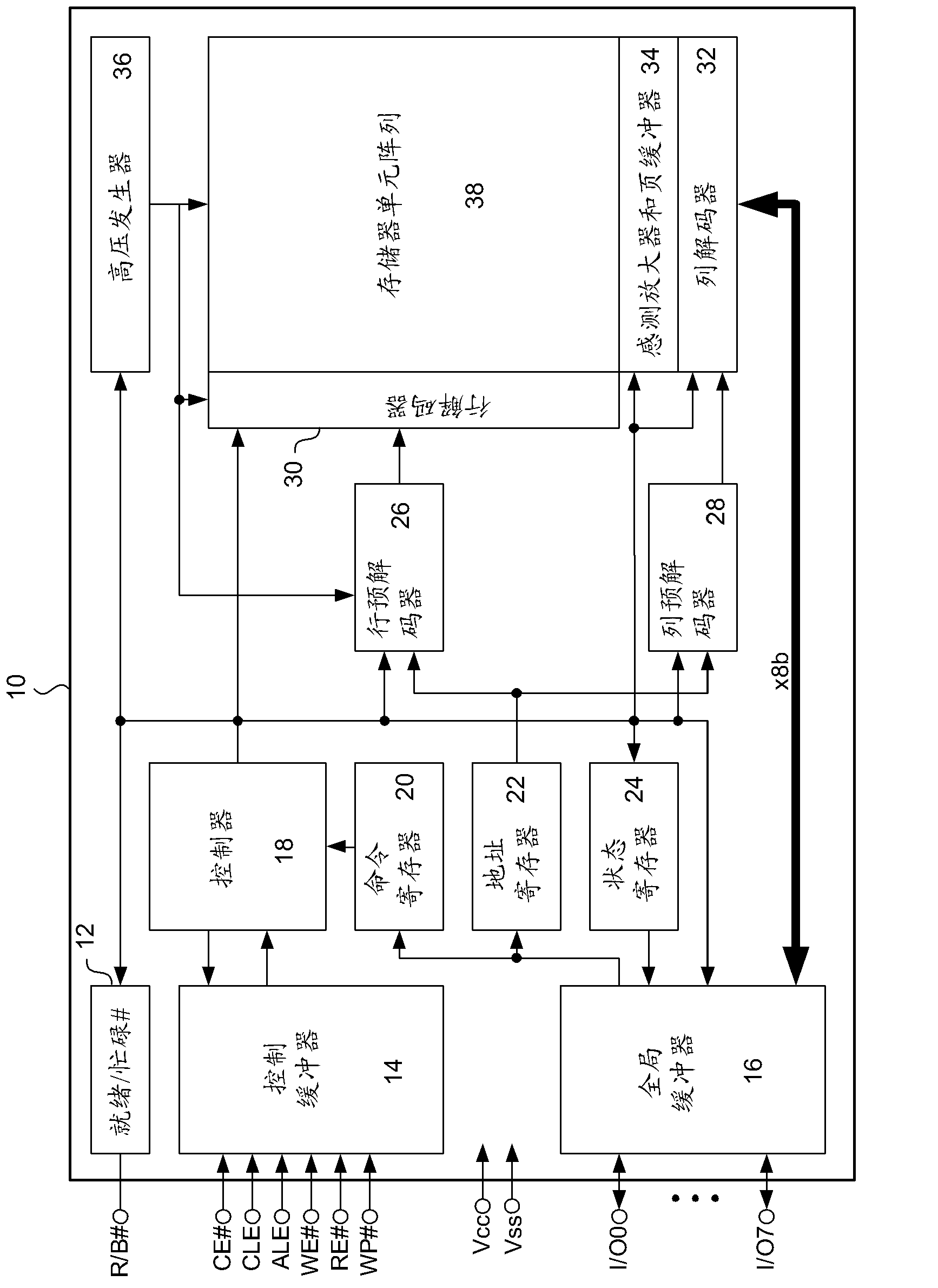
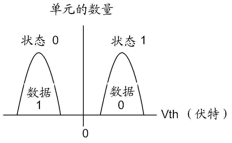
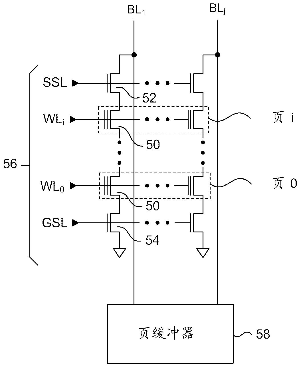
[0071] The present invention generally relates to methods for programming multiple logical pages of data to one physical page of cells in a single programming cycle in flash memory. In particular, circuits and methods are described for programming multiple bits of data to flash memory cells in a single program operation cycle. Multiple pages of data to be programmed into one physical page of the flash memory array are stored in a page buffer or other storage element on the memory device. Selected word lines connected to cells to be programmed are driven at different time intervals using predetermined programming configurations, wherein each predetermined programming configuration is configured to shift the erase threshold voltage to a specific logic state corresponding to a specific threshold voltage. The bit lines are biased to a particular state during each of the time intervals in response to the combination of particular logic states of the bits belonging to each page of ...


PUM


Abstract

A circuit and method for programming multiple bits of data to flash memory cells in a single program operation cycle. Multiple pages of data to be programmed into one physical page of a flash memory array are stored in page buffers or other storage means on the memory device. The selected wordline connected to the cells to be programmed is driven with predetermined program profiles at different time intervals, where each predetermined program profile is configured for shifting an erase threshold voltage to a specific threshold voltage corresponding to a specific logic state. A multi-page bitline controller biases each bitline to enable or inhibit programming during each of the time intervals, in response to the combination of specific logic states of the bits belonging to each page of data that are associated with that respective bitline.

Description

technical field [0001] The present invention relates generally to semiconductor devices, and in particular to programming multiple bits of data into a single flash memory cell. Background technique [0002] Flash memory is a commonly used type of non-volatile memory, which is widely used as a mass memory of consumer electronic products such as digital cameras or portable digital music players. The density of currently available flash memory chips can be as high as several gigabytes (GB) in size, which is suitable for use in common USB flash drives because of the small size of one flash memory chip. Another emerging application of flash memory is solid-state drives, used to replace traditional hard drives used in laptop and desktop computers. [0003] figure 1 is a generalized block diagram of a typical flash memory device known in the art. The flash memory device 10 includes input / output interface circuits, control circuits, memory circuits, and a memory array. The input...

Claims


Application Information

Patent Timeline
Patent Type & Authority Applications(China)
IPC IPC(8): G11C16/10G11C16/24
CPCG11C11/5628G11C16/0483G11C16/10G11C16/24G11C16/34
Inventor 金镇祺
Owner CONVERSANT INTPROP MANAGEMENT INC
Why Eureka
Try Eureka