Color imaging method based on photosensitive composite dielectric gate mosfet detector

A composite medium, color imaging technology, used in picture signal generators, radiation control devices, etc., can solve the problems of color confusion, aggravating color confusion, and affecting imaging quality.

Active Publication Date: 2015-08-19
NANJING UNIV
View PDF7 Cites 0 Cited by
  • Summary
  • Abstract
  • Description
  • Claims
  • Application Information

AI Technical Summary

Problems solved by technology

In this way, the problem of color confusion will be encountered in the process of color restoration, which affects the quality of imaging.
At the same time, as the unit pixel area continues to shrink, the production of color filters will become more and more difficult
Moreover, since the unit pixel area of ​​CCD and CMOS-APS is difficult to continue to shrink, their spatial color sampling frequency cannot be continuously improved, which also aggravates the phenomenon of color confusion.

Method used


Image

  • Color imaging method based on photosensitive composite dielectric gate mosfet detector
  • Color imaging method based on photosensitive composite dielectric gate mosfet detector
  • Color imaging method based on photosensitive composite dielectric gate mosfet detector

Examples


Embodiment Construction

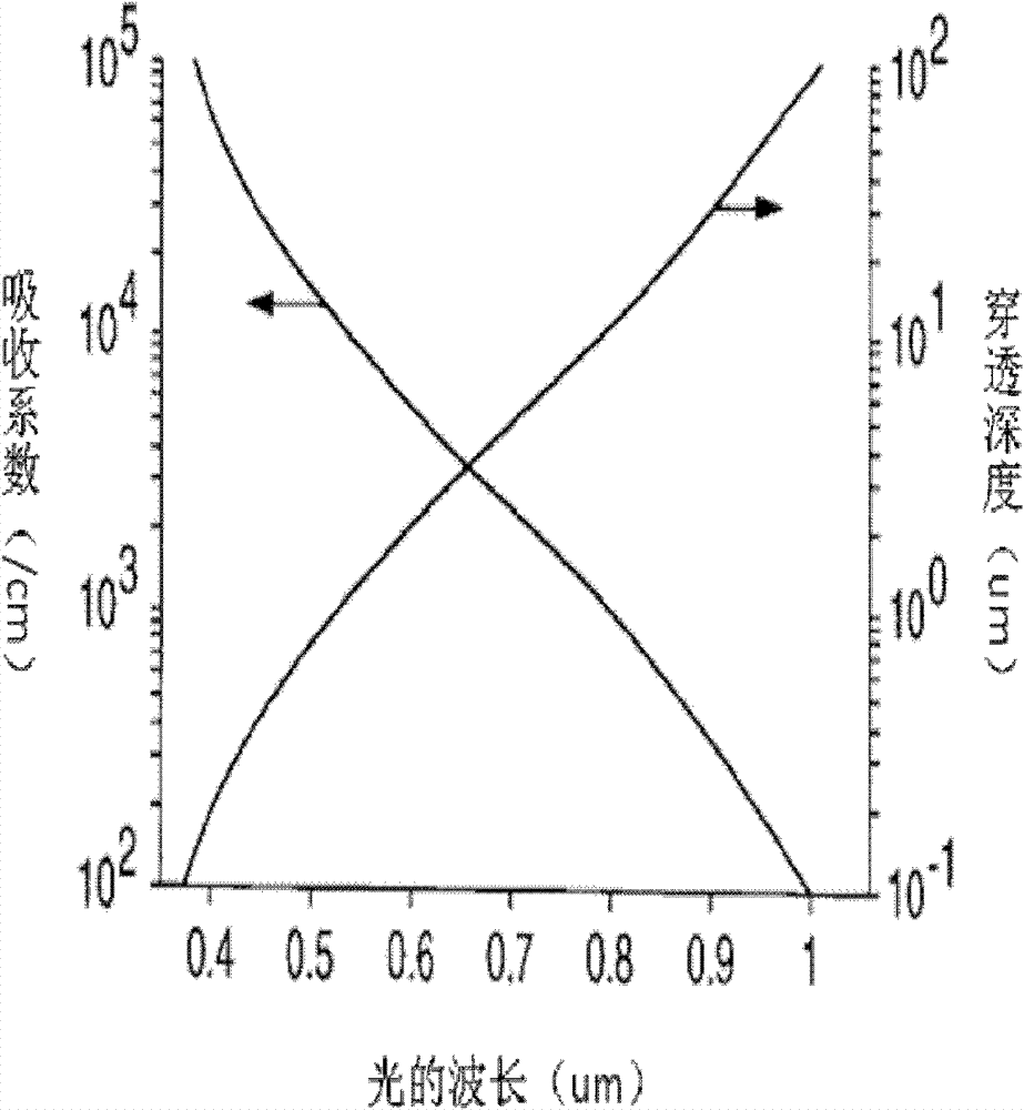
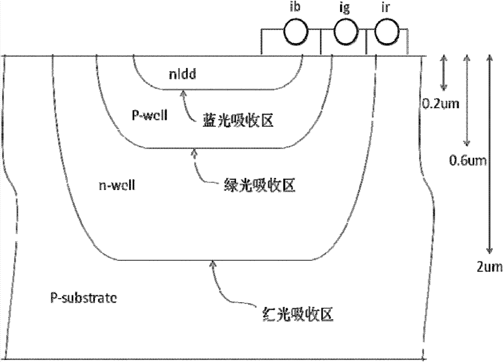
[0050] Incident photons penetrate to different depths in silicon with different wavelengths, figure 1 The penetration depth of light in silicon is shown as a function of wavelength. As shown in the figure, blue light (wavelength of 400-490 nanometers) is mainly absorbed in silicon at a depth of 0.2-0, 5 microns, and green light (wavelength of 490-575 nanometers) is mainly absorbed at 0.5-1.5 microns in silicon. Absorption, red light (wavelength 575 to 700 nanometers) is mainly absorbed in silicon at 1.5 to 3 microns.

[0051]When the voltage applied to the gate of the MOSFET is a pulse voltage, the MOSFET will work in a deep depletion state. At this time, the depletion layer at the interface between the underlying dielectric layer and the P-type silicon substrate will vary with the voltage applied to the gate. Different, the relationship between the depth of the depletion layer and the voltage applied to the gate is as follows:

[0052] W = ...


PUM


Abstract

Then invention provides a color imaging method based on a photosensitive composite medium grid metal oxide semiconductor field effect transistor (MOSFET) detector. According to the color imaging method, different voltage pulses are put on grid electrodes, and the MOSFET works in a deep-exhausting state. According to principles that different grid voltage causes different depths of an exhausting area and lights of different wave lengths has different penetration depth in silicon, red photon, green photon and blue photon in incident light are separated, collected and detected respectively, the three primary colors, namely red, green and blue, are detected in a same pixel to realize color imaging. The color imaging method includes the steps of: imposing a positive pulse Vb on the grid electrodes, forming an exhausting layer of certain depth on a P-type silicon semiconductor to absorb blue light photon, and changing the pulse voltage of the grid electrodes in order to absorb red light photon and blue light photon. The color imaging method has the advantages that color blending phenomenon in traditional color imaging method is avoided, quantum efficiency is improved, technological process is simple, cost is low, and scalability of pixels is good.

Description

technical field [0001] The invention relates to a color imaging method in an imaging detector, in particular to a device structure, working mechanism and operation method for detecting three primary colors (red, green and blue) in the same unit pixel. Background technique [0002] Color imaging methods have extremely important applications in the fields of national defense, medical treatment, monitoring and civilian use. At present, the main color imaging methods can be divided into two categories: 1. According to the principle that different wavelengths of light can penetrate different depths in semiconductor materials, design structures for detection; 2. Use a so-called Bayer color filter array The structure (Bayer color filter array) separates light of different wavelengths for detection. [0003] The first type of technology includes non-imaging devices, which only use different wavelengths of light to penetrate different depths in semiconductor materials to detect ligh...

Claims


Application Information

Patent Timeline
Patent Type & Authority Patents(China)
IPC IPC(8): H01L27/146H04N9/04
Inventor 闫锋卜晓峰胡悦吴福伟夏好广马浩文
Owner NANJING UNIV
Why Eureka
Try Eureka