Simulative switch circuit structure

A technology of analog switch circuit and circuit module, which is applied in the field of analog switch circuit structure, can solve the problems of input signal leaking to the output terminal, etc., achieve stable and reliable working performance, wide application range, and realize the effect of normal shutdown

Active Publication Date: 2013-06-19
CRM ICBG (WUXI) CO LTD
View PDF5 Cites 13 Cited by
  • Summary
  • Abstract
  • Description
  • Claims
  • Application Information

AI Technical Summary

Problems solved by technology

In order to reduce the on-resistance of the circuit, the substrate of the channel PMOS is connected to the input terminal when it is turned on. When this analog switch is powered off, the input signal will also leak to the output terminal.

Method used


Image

  • Simulative switch circuit structure
  • Simulative switch circuit structure
  • Simulative switch circuit structure

Examples


Embodiment approach

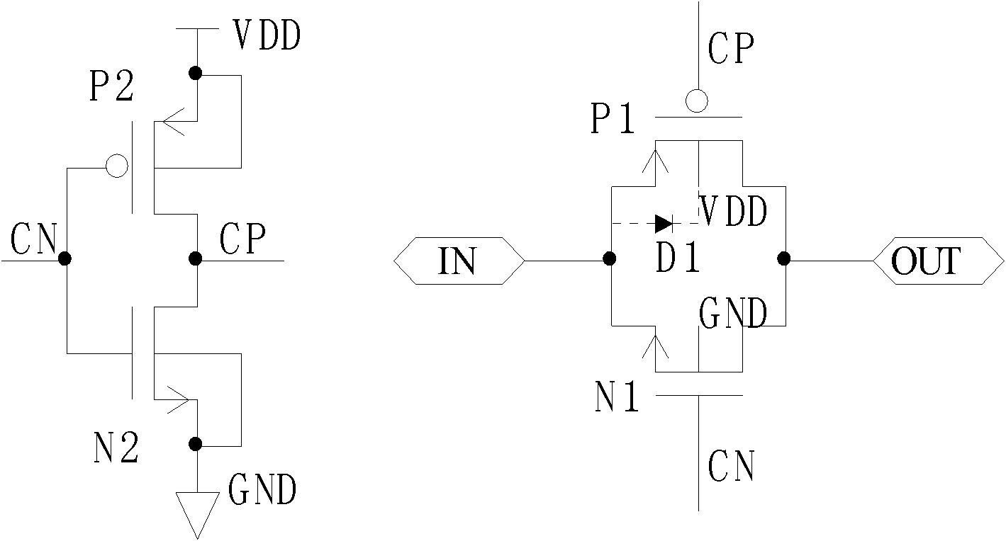
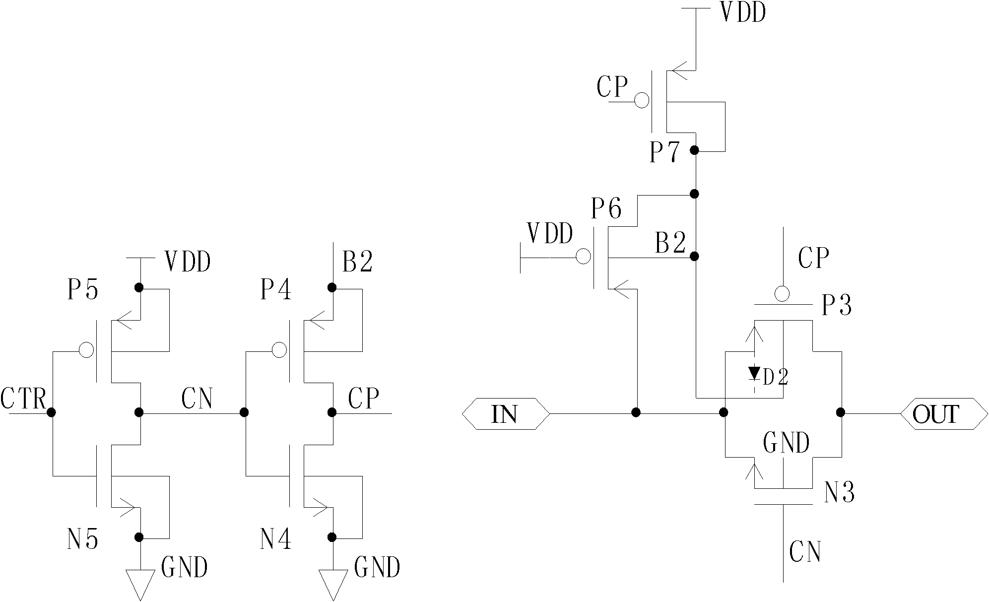
[0033] As a second embodiment of the present invention, the second inverter in the analog switch circuit structure may also include a ninth PMOS field effect transistor P9 and a ninth NMOS field effect transistor N9, and the ninth PMOS field effect transistor The gate of P9 and the gate of the ninth NMOS field effect transistor N9 are both connected to the output terminal CN of the first inverter, and the source and substrate of the ninth PMOS field effect transistor P9 are connected to the power supply VDD connected, the drain of the ninth PMOS field effect transistor P9 is respectively connected with the output terminal CP of the second inverter and the drain of the ninth NMOS field effect transistor N9, and the ninth NMOS field effect transistor Both the substrate and the source of transistor N9 are grounded.

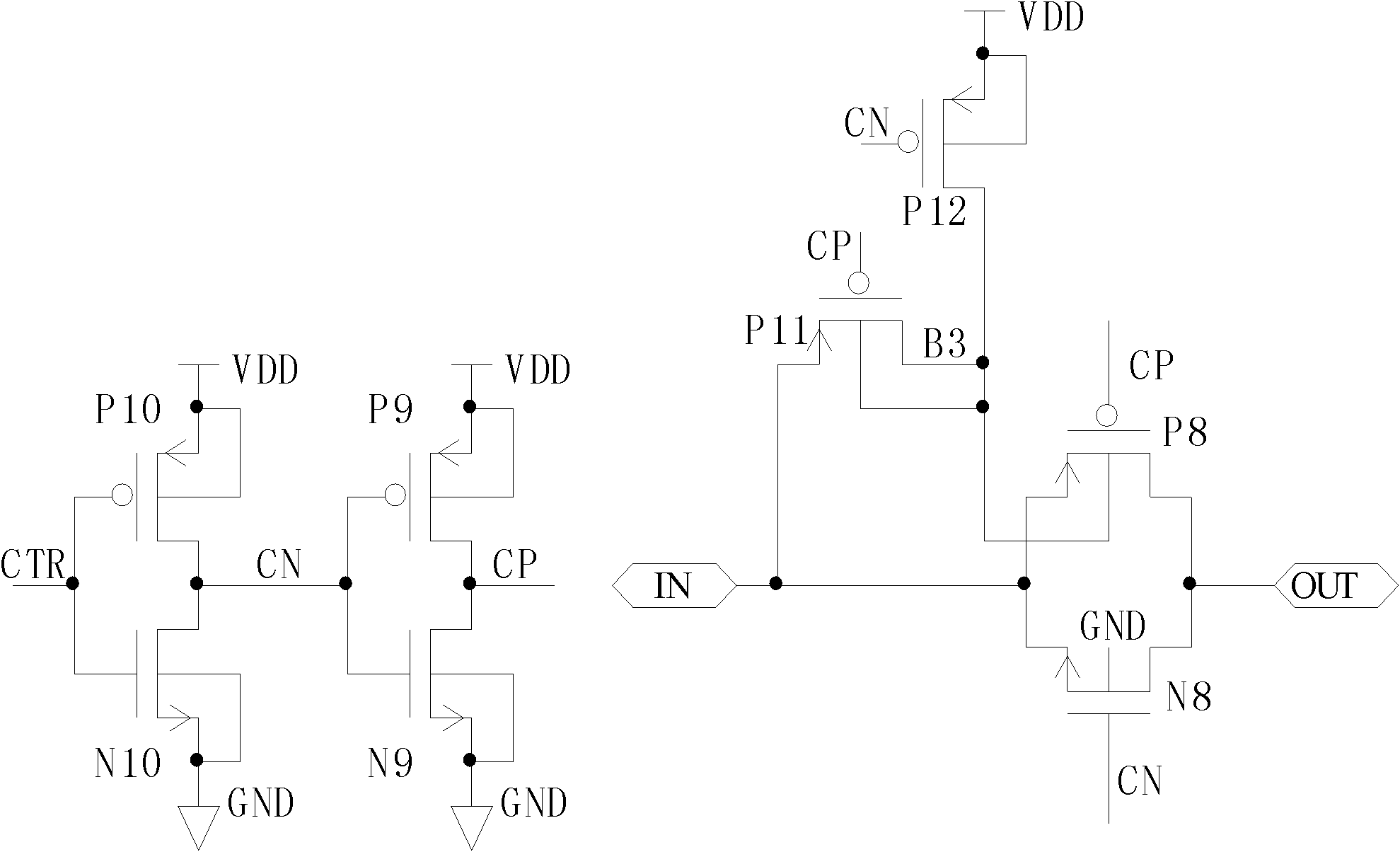
[0034] Wherein, the breakpoint protection circuit module may include an eleventh PMOS field effect transistor P11 and a twelfth PMOS field effect transistor P12, the...


PUM


Abstract

The invention relates to a simulative switch circuit structure. The simulative switch circuit structure comprises a phase inverter circuit module, a passage geminate transistor circuit module and a breaking point protection circuit module, wherein an input end of the phase inverter circuit module is connected with a control signal input terminal (CRT), the passage geminate transistor circuit module is connected between a signal input end (IN) and a signal output end (OUT), the passage geminate transistor circuit module comprises a third P-channel Metal Oxide Semiconductor (PMOS) field effect tube (P3), an output end of the phase inverter circuit module is connected with a grid electrode of the third PMOS field effect tube (P3), and a substrate of the third PMOS field effect tube (P3) is connected with a power source (VDD) or the signal input end (IN) through the breaking point protection circuit module. According to the simulative switch circuit structure, the phenomenon that an input signal leaks power to the VDD through a parasitic diode which is arranged between a field effect tube source electrode and the substrate is avoided, normal turn-off of the simulative switch in a power source power off condition is achieved, the linkage current from the input end to the power source is avoided, and the simulative switch circuit structure is simple in structure, practical, stable and reliable in working performance, and wide in application range.

Description

technical field [0001] The invention relates to the design field of semiconductor integrated circuits, in particular to the technical field of analog switches in semiconductor integrated circuits, and specifically refers to an analog switch circuit structure. Background technique [0002] At present, analog switches are widely used in the transmission and selection of analog signals. The transmission of various high-definition video and audio signals puts forward higher and higher requirements on the performance of analog switches. [0003] In order to transmit a voltage close to the power supply (VDD), the traditional analog switch circuit uses a symmetrical connection between PMOS and NMOS transistors in the transmission channel. The substrate (B end) of the PMOS is connected to VDD, and a parasitic diode is formed between S and B of the PMOS. When VDD is powered off and there is a signal at the input terminal, it will cause the leakage of the parasitic diode from the in...

Claims


Application Information

Patent Timeline
Patent Type & Authority Applications(China)
IPC IPC(8): H03K17/687
Inventor 徐栋叶青朱立群牛征彭云武严淼
Owner CRM ICBG (WUXI) CO LTD
Why Eureka
Try Eureka