
Light-emitting diode package structure

A technology of light-emitting diodes and packaging structures, which is applied to electrical components, electric solid-state devices, circuits, etc., and can solve the problems of light-emitting diodes, such as yellow outside and blue inside

Inactive Publication Date: 2013-06-26
HONG FU JIN PRECISION IND (SHENZHEN) CO LTD +1
View PDF0 Cites 1 Cited by
  • Summary
  • Abstract
  • Description
  • Claims
  • Application Information

AI Technical Summary

Problems solved by technology

The packaging structure of light-emitting diodes often uses blue LED chips and yellow phosphors to produce white light. However, when the light-emitting diodes of this structure are illuminated, the light emitted by the light-emitting diodes appears yellow on the outside and yellow on the inside due to the relatively long path of the light from the outside. The blue problem, commonly known as the yellow halo phenomenon

Method used


Image

  • Light-emitting diode package structure
  • Light-emitting diode package structure

Examples


Embodiment Construction

[0011] The present invention will be further described in detail below in conjunction with the accompanying drawings.

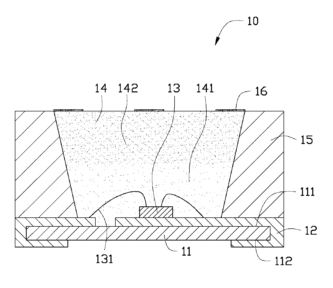
[0012] see figure 1 An LED packaging structure 10 provided in an embodiment of the present invention includes a substrate 11 , electrodes 12 , LED chips 13 , packaging layers 14 , fluorescent particles 141 , diffusing particles 142 , reflective cups 15 and light-shielding particles 16 .

[0013] The substrate 11 is a rectangular flat plate for supporting the electrodes 12 , the LED chips 13 and the encapsulation layer 14 thereon. The substrate 11 includes an upper surface 111 and a lower surface 112 opposite to the upper surface 111 and parallel to each other. The substrate 11 is made of insulating materials such as PPA (Polyphthalamide, polyvinyl acetate). It can be understood that the lengths of the sides of the substrate 11 may be the same or different. Further, the shape of the substrate 11 is not limited to a rectangle, and may also be a circle or the ...


PUM

PropertyMeasurementUnit
The average particle sizeaaaaaaaaaa

Abstract

A light-emitting diode package structure comprises a substrate, two electrodes arranged on the substrate, a light-emitting diode chip electrically connected with the electrodes, a package layer, fluorescent particles and diffusion particles. The fluorescent particles and the diffusion particles are mixed in the package layer. The average particle size of the diffusion particles is smaller than the average particle size of the fluorescent particles. Density of the diffusion particles at the position far away from the light-emitting diode chip is larger than the density of the diffusion particles at the position close to the light-emitting diode chip, and the density of the fluorescent particles at the position close to the light-emitting diode chip is larger than the density of the fluorescent particles at the position far away from the light-emitting diode chip.

Description

technical field [0001] The invention relates to a semiconductor package structure, in particular to a light emitting diode package structure. Background technique [0002] As the third-generation light source, light-emitting diodes have the advantages of small size, energy saving and environmental protection, and high luminous efficiency, and have been more and more widely used. The packaging structure of light-emitting diodes often uses blue LED chips and yellow phosphors to produce white light. However, when the light-emitting diodes of this structure are illuminated, the light emitted by the light-emitting diodes appears yellow on the outside and yellow on the inside due to the relatively long path of the light from the outside. The problem of blue is commonly known as the yellow halo phenomenon. Contents of the invention [0003] In view of this, it is necessary to provide a light emitting diode packaging structure that can reduce the yellow halo phenomenon. [0004]...

Claims


Application Information

Patent Timeline
IPC IPC(8): H01L33/48H01L33/58H01L33/50
CPCH01L2224/48091
Inventor 曾坚信
Owner HONG FU JIN PRECISION IND (SHENZHEN) CO LTD
Learn More