Packaged semiconductor device and method of packaging the semiconductor device

A technology of semiconductor and semiconductor tube, applied in the field of semiconductor packaging

Active Publication Date: 2013-07-03
TAIWAN SEMICON MFG CO LTD
View PDF3 Cites 24 Cited by
  • Summary
  • Abstract
  • Description
  • Claims
  • Application Information

AI Technical Summary

Problems solved by technology

These relatively new packaging technologies...

Method used


Image

  • Packaged semiconductor device and method of packaging the semiconductor device
  • Packaged semiconductor device and method of packaging the semiconductor device
  • Packaged semiconductor device and method of packaging the semiconductor device

Examples


Embodiment Construction

[0037] The making and using of embodiments of the invention are discussed in detail below. It should be appreciated, however, that the present invention provides many applicable inventive concepts that can be embodied in a wide variety of specific contexts. The specific embodiments discussed are merely illustrative of specific ways to make and use the invention, and do not limit the scope of the invention.

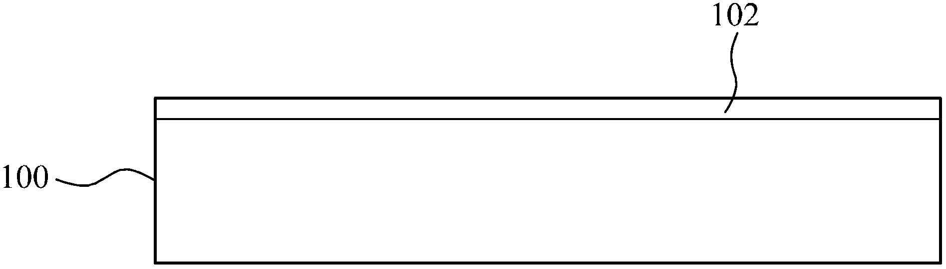
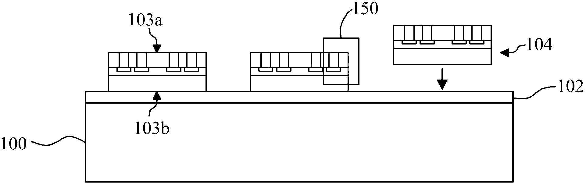
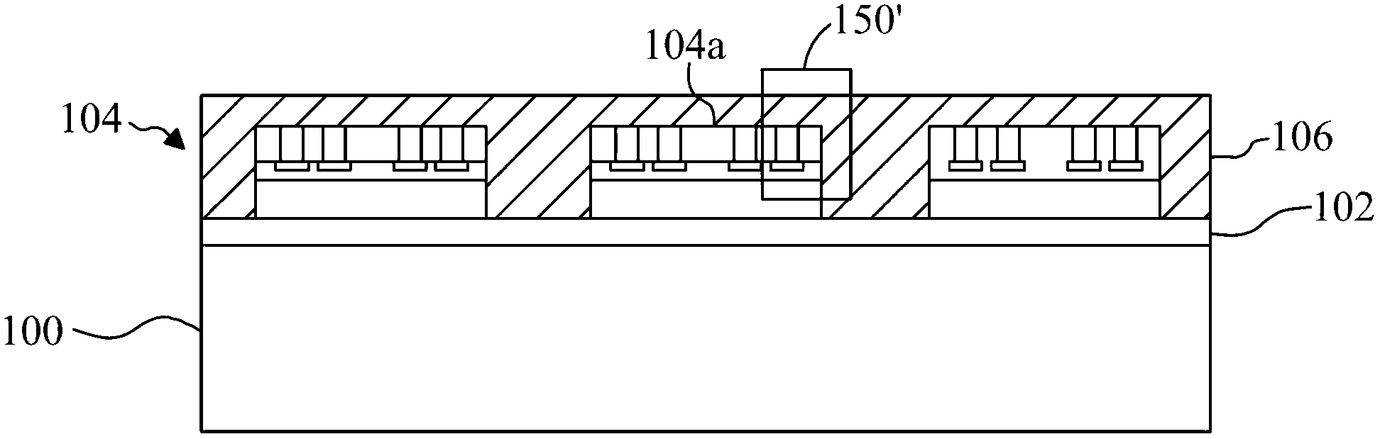
[0038] Figure 1A to Figure 1I are cross-sectional views of a semiconductor device at various packaging stages according to an embodiment of the present invention. first reference Figure 1A , a carrier wafer 100 is provided. As examples, carrier wafer 100 may comprise glass, silicon oxide, aluminum oxide, and the like. The thickness of the carrier wafer 100 may range from about a few mils to tens of mils, and may include a diameter of about 300 mm in some embodiments. The carrier wafer 100 serves as a packaged semiconductor device or die 104 (see Figure 1B ) functi...


PUM

PropertyMeasurementUnit
Thicknessaaaaaaaaaa

Abstract

The mechanisms of forming a molding compound on a semiconductor device substrate to enable fan-out structures in wafer-level packaging (WLP) are provided. The mechanisms involve covering portions of surfaces of an insulating layer surrounding a contact pad. The mechanisms improve reliability of the package and process control of the packaging process. The mechanisms also reduce the risk of interfacial delamination, and excessive outgassing of the insulating layer during subsequent processing. The mechanisms further improve planarization end-point. By utilizing a protective layer between the contact pad and the insulating layer, copper out-diffusion can be reduced and the adhesion between the contact pad and the insulating layer may also be improved.

Description

[0001] Cross References to Related Applications [0002] This application is related to the following co-pending and commonly assigned patent application: Serial titled "Packaging Methods and Structures Using a Die Attach Film," filed September 8, 2011 Serial No. 13 / 228,244, the entire contents of which are incorporated into this application. technical field [0003] The present invention relates to semiconductor packaging, and in particular, to a packaged semiconductor device and a method of packaging a semiconductor device. Background technique [0004] Semiconductor devices are used in various electronic applications, such as personal computers, cell phones, digital cameras, and other electronic equipment. Semiconductor devices are generally fabricated by sequentially depositing insulating or dielectric layers, conductive layers, and semiconductive layers of materials over a semiconductor substrate, and patterning the various material layers using photolithography to for...

Claims


Application Information

Patent Timeline
IPC IPC(8): H01L23/498H01L21/48
CPCH01L24/19H01L24/20H01L2224/04105H01L23/3128H01L21/561H01L21/568H01L2924/181H01L2924/12042H01L2224/12105H01L23/3114H01L2224/96H01L2924/00H01L21/56H01L21/78H01L24/03H01L24/82H01L2224/0231H01L2224/821
Inventor 林俊成洪瑞斌刘乃玮茅一超施婉婷董簪华
Owner TAIWAN SEMICON MFG CO LTD
Why Eureka
Try Eureka