Semiconductor interconnect structure and method of forming

An interconnection structure and semiconductor technology, which is applied in semiconductor devices, semiconductor/solid-state device manufacturing, semiconductor/solid-state device components, etc., can solve the problems of semiconductor manufacturing process mismatch, high production cost, and complex formation process, etc., to avoid Effects of breaking, increasing mechanical strength, and preventing shrinkage

Active Publication Date: 2016-01-06
SEMICON MFG INT (SHANGHAI) CORP
View PDF11 Cites 0 Cited by
  • Summary
  • Abstract
  • Description
  • Claims
  • Application Information

AI Technical Summary

Problems solved by technology

[0006] However, the formation process of the above-mentioned prior art is complicated, does not match the existing semiconductor manufacturing process, and the production cost is high

Method used


Image

  • Semiconductor interconnect structure and method of forming
  • Semiconductor interconnect structure and method of forming
  • Semiconductor interconnect structure and method of forming

Examples


Embodiment Construction

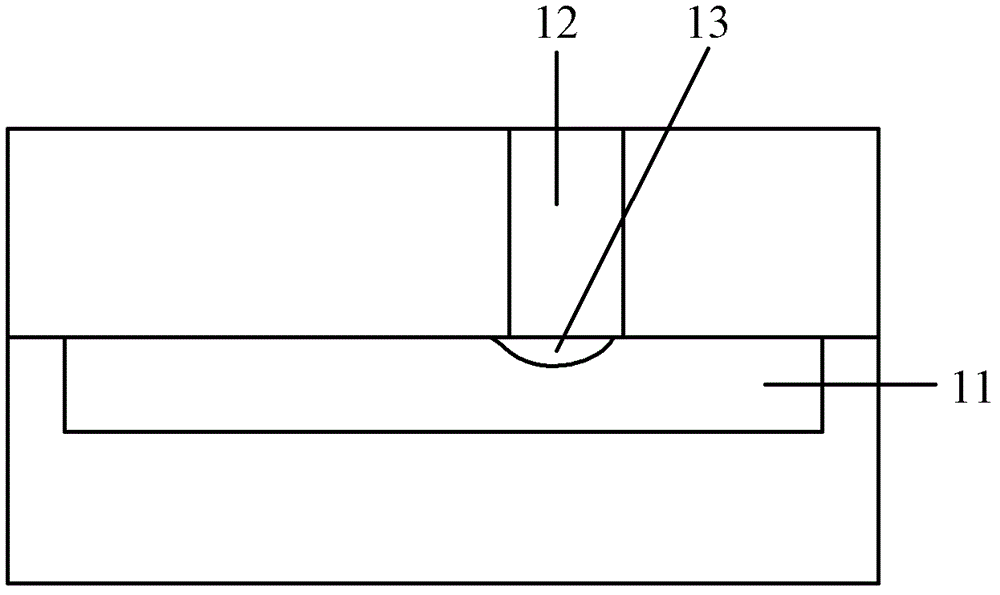
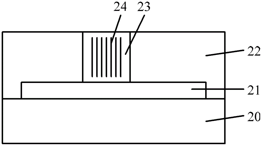
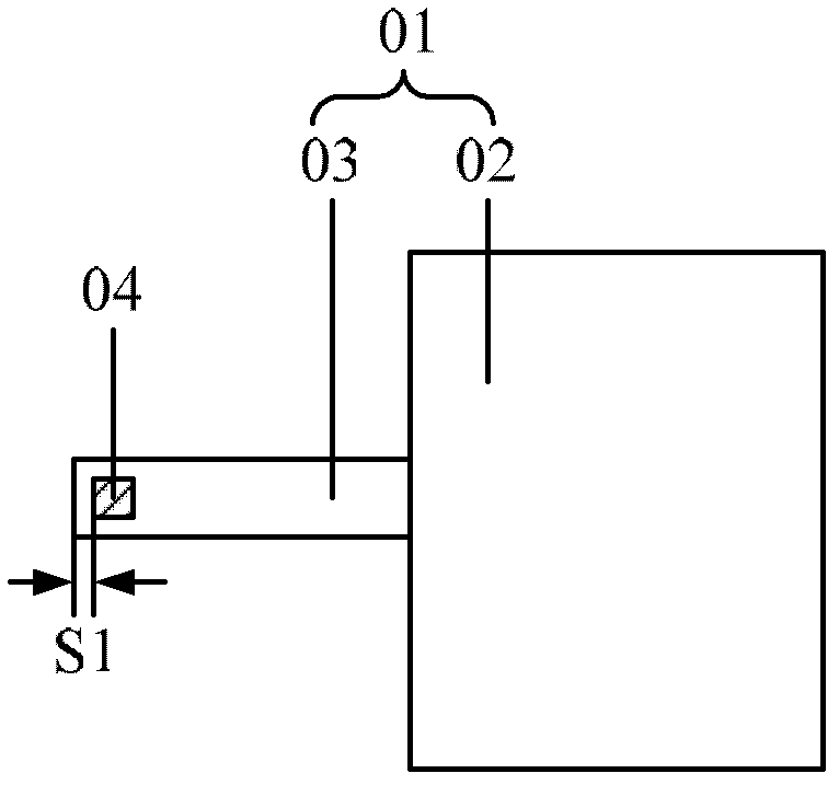
[0038] Due to the complex formation process of the prior art mentioned in the background art, which does not match the existing semiconductor manufacturing process, and high production costs, the inventors found that the vacancies used to form voids are in the form of through-silicon vias and metal interconnection layers. The contact position is formed in the circular metal layer at the center of the circle. If the area of ​​the metal interconnection layer is small, the number of vacancies formed by tensile stress is small, and the probability of forming voids will be greatly reduced. Therefore, the invention proposed a semiconductor interconnection structure, please refer to image 3 , is a schematic structural diagram of the semiconductor interconnection structure of this embodiment, including: a metal interconnection layer 01, the metal interconnection layer 01 includes a metal layer 02 and a metal protrusion 03 connected to the edge of the metal layer 02; The conductive pl...


PUM


Abstract

The invention discloses an interconnection structure of semiconductors and a formation method. The interconnection structure of the semiconductors comprises a metal interconnecting layer including a metal layer and a first metal protrusion connected with the edges of the metal layer and a conductive plug arranged on the surface of the first metal protrusion, wherein the distance between the conductive plug and the point of the first metal protrusion is larger than the minimum design size. When the temperature of the semiconductor interconnection structure drops from high manufacturing technique temperature to room temperature, the portions, corresponding to the parts from the conductive plug to the point of the first metal protrusion and from the conductive plug to the metal edge, of the first metal protrusion shrink, produced stresses are cancelled out, and thus the positions of the conductive plug and the metal protrusion do not missed relatively, and no gaps are formed at the contacting position of the conductive plug and the metal protrusion.

Description

technical field [0001] The invention relates to semiconductor technology, in particular to a semiconductor interconnection structure and a forming method capable of reducing interconnection layer stress migration. Background technique [0002] With the advancement of semiconductor technology, the size of integrated circuits has become smaller and smaller. When the integration of integrated circuits increases, the surface of the chip cannot provide enough area to make the required interconnection lines. Therefore, most of the current VLSI structures use a multi-layer stacked metal interconnection structure. [0003] In the multi-layer stacked metal interconnection structure, each layer of metal interconnection layer includes several metal interconnection lines, and the metal interconnection lines in the same layer are separated by dielectric materials, and the metal interconnection lines in different layers The wires are also separated by dielectric materials, and the metal ...

Claims


Application Information

Patent Timeline
Patent Type & Authority Patents(China)
IPC IPC(8): H01L23/528H01L21/768
Inventor 甘正浩
Owner SEMICON MFG INT (SHANGHAI) CORP
Why Eureka
Try Eureka