Testing structure, forming method of testing structure and washing time judging method of washing process

A technology of test structure and judgment method, which is applied in semiconductor/solid-state device testing/measurement, electrical components, electric solid-state devices, etc., can solve the problems of semiconductor device yield decline, thin-film material property degradation, and inability to detect manufacturing processes, etc., to achieve Form the effect of simple process

Active Publication Date: 2013-07-03
SEMICON MFG INT (SHANGHAI) CORP
View PDF8 Cites 3 Cited by
  • Summary
  • Abstract
  • Description
  • Claims
  • Application Information

AI Technical Summary

Problems solved by technology

[0003] When the distribution of stress in the thin films on the surface of the wafer is not uniform, or when an inappropriate external force is applied to the thin films on the wafer surface, excessive film stress will be generated locally on the wafer. This excessive film stress It often leads to serious degradation of the properties of thin film materials, such as cracks on the surface of local wafers, which in turn leads to a decrease in the yield of subsequent semiconductor devices and affects the performance of integrated circuits
[0004] The Chinese patent with the publication number "CN1229913A" discloses a "method and device for measuring internal film s

Method used


Image

  • Testing structure, forming method of testing structure and washing time judging method of washing process
  • Testing structure, forming method of testing structure and washing time judging method of washing process
  • Testing structure, forming method of testing structure and washing time judging method of washing process

Examples


example 1

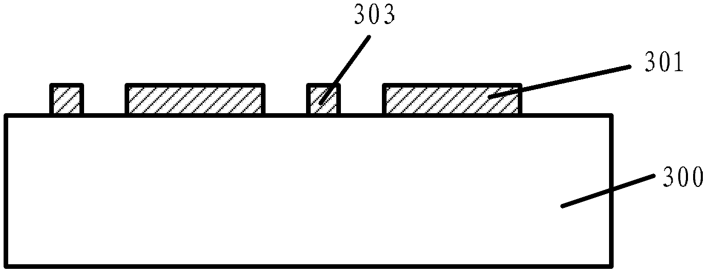
[0067] Please refer to Figure 6 , the long side of the first pattern 301 is greater than 100 microns, the short side is greater than 25 microns, the long side of the second pattern 303 is greater than 100 microns, and the short side is greater than 25 microns, the first pattern 301 and the second pattern 303 The distance between them is less than or equal to 5 microns.

[0068] In Example 1 of the present invention, the long side of the first pattern 301 is 150 microns, the short side is 100 microns, the long side of the second pattern 303 is 110 microns, and the short side is 80 microns, the first The distance between the pattern 301 and the second pattern 303 is 3 microns. In the test structure formed subsequently in Example 1, cracks are more likely to appear in the corresponding areas between the first pattern 301 and the second pattern 303 .

example 2

[0070] Please refer to Figure 7 , the long side of the first pattern 301 is greater than 100 microns, the short side is greater than 25 microns, the area of ​​the second pattern 303 is less than 1 square micron, and the distance between the first pattern 301 and the second pattern 303 is less than or equal to 5 microns.

[0071] In Example 1 of the present invention, the long side of the first pattern 301 is 150 microns, the short side is 100 microns, the long side of the second pattern 303 is 0.8 microns, and the short side is 0.5 microns, the first The distance between the pattern 301 and the second pattern 303 is 2 microns. In the test structure formed subsequently in Example 2, cracks are more likely to appear in the corresponding areas between the first pattern 301 and the second pattern 303 . Since the distance between the first graphic 301 and the second graphic 303 in Example 2 is small, cracks are more likely to appear in the corresponding areas between the first g...


PUM

PropertyMeasurementUnit
Thicknessaaaaaaaaaa
Thicknessaaaaaaaaaa
Thicknessaaaaaaaaaa

Abstract

Provided is a testing structure. The testing structure comprises a substrate, a pattern layer placed on the surface of the substrate, and a detection layer placed on the surface of the pattern layer. The pattern layer at least comprises a first pattern and a second pattern, the area of the first pattern or the area of the second pattern is at least larger than 2500 square microns, and the distance between the first pattern and the second pattern is equal to or smaller than a corresponding design rule. Meanwhile, the invention further provides a forming method of the testing structure and a washing time judging method of washing process by adopting the testing structure. With the methods, proper parameters of manufacturing process can be found, yields of semiconductor devices can be improved, and performance of integrated circuits can be improved.

Description

technical field [0001] The invention relates to the technical field of semiconductor manufacturing, in particular to a test structure and its forming method, and a method for judging the flushing time of the flushing process. Background technique [0002] Current semiconductor fabrication techniques typically employ more than one thin film layer (eg, a multi-layer stack) in order to impart more features to an integrated circuit (IC) chip. Usually, due to the characteristics of the film materials of each layer (such as elasticity, thermal expansion, etc.) and the shape, size and distribution of the graphics on each layer of film are different, stress will be generated inside each layer of film. Moreover, external forces in the manufacturing process (such as temperature rise and fall, impact of high-pressure water column, mechanical pressure and vacuum adsorption, etc.) will also affect the distribution of stress in the films of each layer on the wafer surface. [0003] When ...

Claims


Application Information

Patent Timeline
IPC IPC(8): H01L23/544H01L21/02H01L21/66
Inventor 柳会雄林爱梅
Owner SEMICON MFG INT (SHANGHAI) CORP
Why Eureka
Try Eureka