Drive control unit, drive circuit and drive control method of display substrate

A display substrate and display driver technology, which is applied to static indicators, instruments, etc., can solve the problems of different charging effects of pixels, the influence of image consistency, and large signal line impedance, and achieve the effect of ensuring the consistency of charging effects

Active Publication Date: 2013-07-10
BOE TECH GRP CO LTD +1
View PDF6 Cites 60 Cited by
  • Summary
  • Abstract
  • Description
  • Claims
  • Application Information

AI Technical Summary

Problems solved by technology

[0003] Due to the limitation of the process characteristics of the liquid crystal panel, there is a certain impedance between the signal lines connecting the near point and the far point, which causes the gate driver and the source driver to load the same signal. The performance of the pixels is inconsistent, so that when the same timing control signal is used for the near point and the far point, the actual

Method used


Image

  • Drive control unit, drive circuit and drive control method of display substrate
  • Drive control unit, drive circuit and drive control method of display substrate
  • Drive control unit, drive circuit and drive control method of display substrate

Examples


Embodiment 1

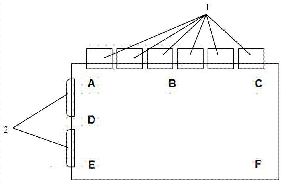
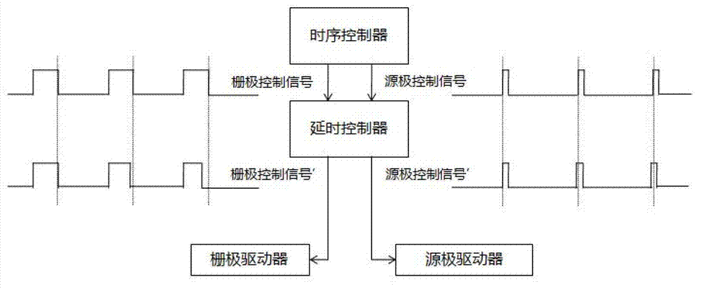
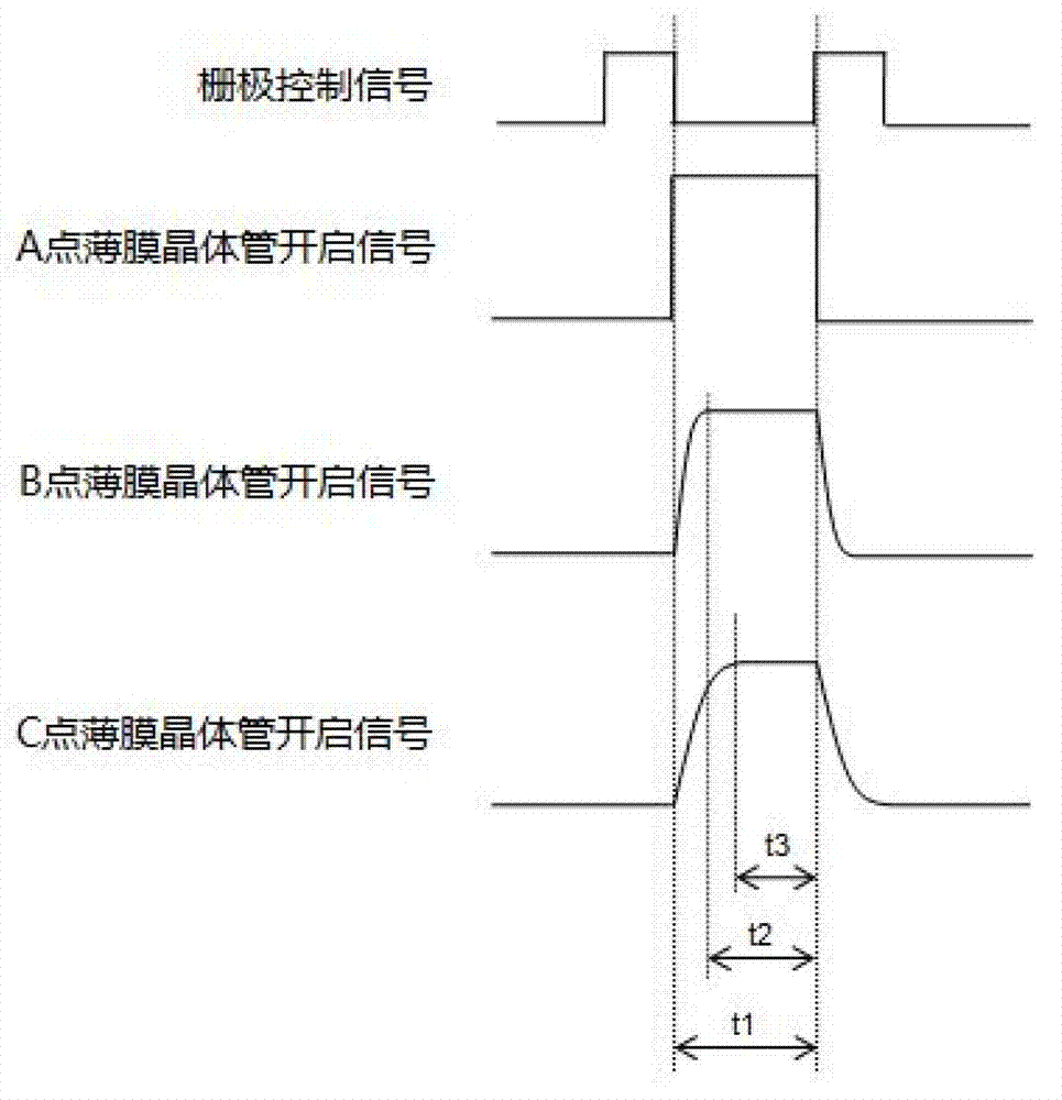
[0054] Such as figure 1 As shown, if the scanning order of the gate lines and data lines on the LCD panel is from left to right and from top to bottom, the pixel point F in the last row and the last column on the LCD panel is the same as the pixel point F in the first row and the first row on the LCD panel. The charging time difference of pixel point A in one column is the largest, therefore, preferably, the delay controller adjusts based on the timing control signal of the pixel point F farthest from the source driver and the gate driver on the liquid crystal panel, The preferred adjustment method is as follows:

[0055] According to the difference between the impedance of the driving signal line connected between the second pixel point on the display substrate and the pixel display driver and the impedance of the driving signal line connected between the first pixel point and the pixel display driver The value is adjusted according to the difference between the impedance of...

Embodiment 2

[0060] Such as figure 1 As shown, the charging time difference between the pixel point F in the last row and the last column on the LCD panel and the pixel point A in the first row and the first column on the LCD panel is the largest, and the delay controller is based on the distance between the source driver and the gate on the LCD panel. The timing control signal of the farthest pixel point F of the pole driver is used as a reference, and the delay of the timing control signal of the pixel point in the same column as the pixel point F is adjusted according to the impedance difference between the pixel point F and the pixels in the same column Time, the impedance difference between pixel point C and pixel far point F is the largest, it is necessary to adjust the delay time of the timing control signal of the row where pixel point C is located, so that the timing control signal of the row where pixel point C is located is later than that of the row where pixel point F is locate...

Embodiment 3

[0062] The delay controller adjusts the timing control signal based on the timing control signal of the pixel point C on the same row of the liquid crystal panel farthest from the gate driver, and according to the impedance difference between the pixel point C and the pixel point A and B of the same row The value adjusts the delay time of the timing control signal of the pixel point in the same row as the pixel point farthest from the gate driver in each row. The difference in impedance between pixel point A and pixel point C is the largest, and the timing of the column where pixel point A is located needs to be adjusted. The delay time of the control signal makes the output of the timing control signal of the column where the pixel point A is located later than the timing control signal of the column where the pixel point C is located, so as to compensate for the fact that the control signal of the gate driver between the pixel points A and C is on the glass substrate trace De...


PUM


Abstract

The invention discloses a drive control unit, a drive circuit and a drive control method of a display substrate. The drive control unit comprises a time schedule controller and a delay controller, wherein time schedule controller sends sequential control signals to the delay controller, the delay controller is used for regulating the sequential control signals according to impedance of a drive signal wire connected with pixel points of the display substrate, and real charge duration of the pixel points is within a preset duration range. According to the drive control unit, the drive circuit and the drive control method, the sequential control signals of the pixel points are changed according to positions of the pixel points on a liquid crystal panel, the sequential control signals of pixel points in different positions are different, charge time errors caused by signal wire delay are compensated by the different sequential control signals, and consistency of charge effects of the pixel points in the different positions of the liquid crystal panel is guaranteed.

Description

technical field [0001] The invention belongs to the field of display technology, in particular to a drive control unit, a drive circuit and a drive control method of a display substrate. Background technique [0002] The traditional liquid crystal panel driving architecture includes a source driver and a gate driver. When the source driver and the gate driver drive pixels at different positions on the panel, the timing control signals used are consistent, that is, the distance between the source driver and the gate driver The near point and far point pixels use the same timing control signal. When the gate driver drives the pixels of each row, the time for loading the deflection voltage on the data line is fixed, and the pixels at different positions in the same row of pixels are turned on. The time is fixed. [0003] Due to the limitation of the process characteristics of the liquid crystal panel, there is a certain impedance between the signal lines connecting the near po...

Claims


Application Information

Patent Timeline
IPC IPC(8): G09G3/36
CPCG09G3/3611G09G2310/08G09G2320/0223
Inventor 段欣
Owner BOE TECH GRP CO LTD
Why Eureka
Try Eureka