Pixel element structure and non-refrigeration infrared focal plane detector based on pixel element structure

A pixel structure and pixel technology, applied in the field of infrared detection, can solve the problems of high equipment cost, long development cycle, complex device manufacturing process, etc., and achieve the effects of easy high-speed response, simplified process difficulty, and low thermal conductivity

Inactive Publication Date: 2013-07-10
孙健 +1
View PDF6 Cites 14 Cited by
  • Summary
  • Abstract
  • Description
  • Claims
  • Application Information

AI Technical Summary

Problems solved by technology

As a result, the manufacturing process of the device is more complicated, and the yield rate is difficult to increase. At the same time, there are problems such as high equipment cost, large investment in research and development and production, and long development cycle.

Method used


Image

  • Pixel element structure and non-refrigeration infrared focal plane detector based on pixel element structure
  • Pixel element structure and non-refrigeration infrared focal plane detector based on pixel element structure
  • Pixel element structure and non-refrigeration infrared focal plane detector based on pixel element structure

Examples


Embodiment 1

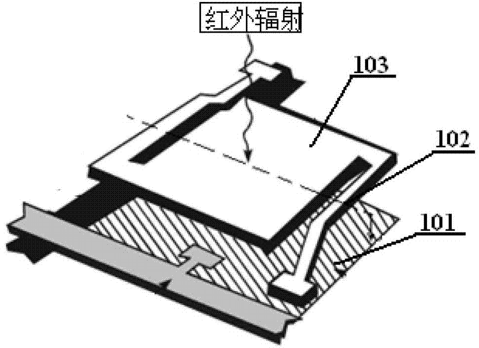
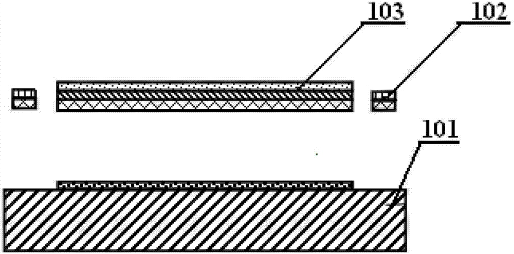
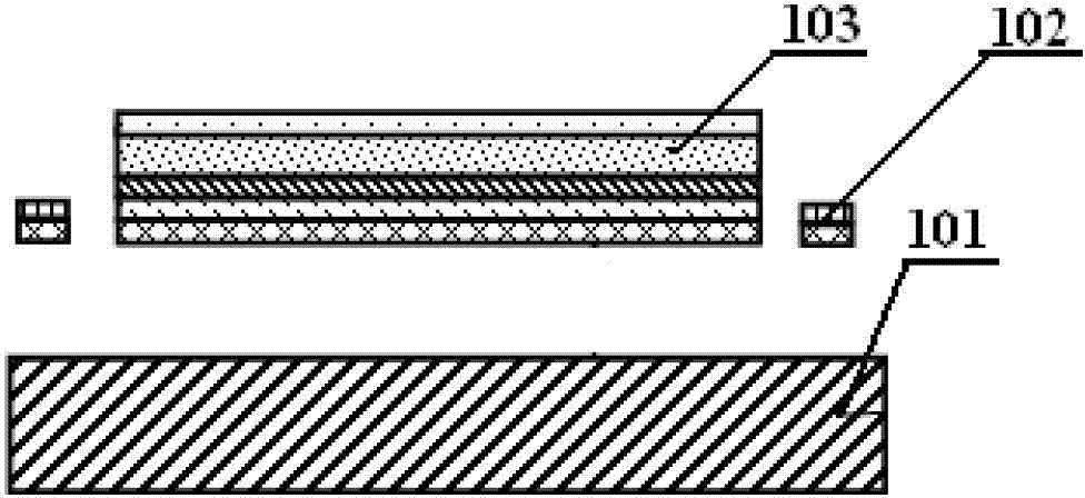
[0037] see Figure 1-8 A pixel structure provided by Embodiment 1 of the present invention includes: a silicon substrate 101, an absorbing unit for absorbing light beams, a conductive unit for connecting the silicon substrate 101 and the absorbing unit, and a conductive unit for converging the radiation beam into the light concentrating unit of the silicon substrate 101. Wherein, a light-transmitting area is provided at the center of the upper surface of the silicon substrate 101, and a readout circuit 110 is provided on the same surface near the periphery of the light-transmitting area; one end of the conductive unit is electrically connected to the absorbing unit, and the other end is connected to the readout circuit 110. The contact electrodes are electrically connected. The absorbing unit is suspended on the upper surface of the silicon substrate 101 through the conductive unit, and the light concentrating unit 104 is fixed on the lower surface of the silicon substrate 10...

Embodiment 2

[0056] see Figure 9-10, Embodiment 2 of the present invention provides an uncooled infrared focal plane detector based on the above pixel structure, including: a first substrate 201 (active board) and a second substrate 202 (passive board). Wherein, one side of the first substrate 201 is provided with at least one light-transmitting area, and the same surface is provided with a readout circuit 110 near the periphery of the light-transmitting area, and the other side is provided with a light-collecting unit 104, and the light-transmitting area is on one side of the first substrate 201 Distributed in an array, the distribution shape of the concentrating units 104 on the other side of the first substrate 201 is adapted to the shape of the pixels in the light-transmitting area; that is, the first substrate 201 is provided with a densely arranged "pixel structure" array, each The central part of the "pixel structure" is provided with a light-transmitting area on one side of the fi...


PUM


Abstract

The invention discloses a pixel element structure and a non-refrigeration infrared focal plane detector based on the pixel element structure. The pixel element structure comprises a silicon substrate, an absorption unit, a conductive unit and a condensation unit which is used for collecting radiation beams and irradiating the radiation beams into the silicon substrate, wherein the condensation unit is fixed on the lower surface of the silicon substrate; a light-transmitting area is arranged in the center of the upper surface of the silicon substrate, and a reading circuit is arranged on a same face, close to the peripheral position of the light-transmitting area, of the light-transmitting area; and one end of the conductive unit is electrically connected with the absorption unit, and the other end of the conductive unit is electrically connected with a contact electrode of the reading circuit. The absorption unit is suspended on the upper surface of the silicon substrate through the conductive unit. Meanwhile, a first substrate integrated with the pixel element structure, and a second substrate provided with a cavity and a through hole array are fixed in a bonding mode to constitute the non-refrigeration infrared focal plane detector, the purpose that fill factors reach as high as 90%-100% is achieved, and the infrared focal plane detector has the advantages of being lower in heat conduction, faster in response speed, and simpler in manufacturing process.

Description

technical field [0001] The invention belongs to the technical field of infrared detection, in particular to a pixel structure and an uncooled infrared focal plane detector based on the pixel structure. Background technique [0002] The uncooled infrared focal plane device (IRFPA) is the core component of the uncooled infrared imaging detection system, which has a wide range of applications in the imaging fields of infrared and terahertz (THz) bands. With the advancement of technology and the improvement of imaging performance requirements, IRFPA is developing towards the direction of large array, small pixel area, low power consumption and high sensitivity. The current maximum number of arrays of IRFPA has reached 1024×768, and the pixel area is 17 ×17μm 2 , further efforts are being made towards 12×12μm 2 step forward. Reducing the pixel area can reduce the chip area of ​​the array device, increase the number of chips on the wafer, increase the yield rate of the wafer, a...

Claims


Application Information

Patent Timeline
Patent Type & Authority Applications(China)
IPC IPC(8): H01L27/144G01J5/20
Inventor 孙健李明燃
Owner 孙健
Why Eureka
Try Eureka