Two-color infrared detector material and preparation method thereof

An infrared detector and epitaxy technology, which is applied in the field of materials, can solve the problems of reduced contrast and difficult identification of infrared targets, and achieves the effects of reducing detection limitations, improving resolution, and improving detection effects.

Active Publication Date: 2013-07-17
11TH RES INST OF CHINA ELECTRONICS TECH GROUP CORP
View PDF2 Cites 7 Cited by
  • Summary
  • Abstract
  • Description
  • Claims
  • Application Information

AI Technical Summary

Problems solved by technology

[0002] Infrared detectors have been widely used in early warning satellites, missile detection, lidar, communications, night vision, and infrared imaging due to their excellent performance. However, with the continuous development of existing infrared detectors, infrared stealth technology is also ...

Method used


Image

  • Two-color infrared detector material and preparation method thereof
  • Two-color infrared detector material and preparation method thereof

Examples


Embodiment 1

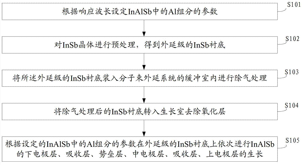
[0045] Embodiments of the present invention provide a method for preparing a two-color infrared detector material, such as figure 1 As shown, the method includes:

[0046] S101, setting the parameters of the Al component in InAlSb according to the response wavelength;

[0047] The response wavelength includes MW 1 band and MW 2 band, the wavelength range corresponding to the MW 1 band is 3.4-4.0 μm, and the wavelength range corresponding to the MW 2 band is 4.4-5.0 μm.

[0048] S102, pretreating the InSb crystal to obtain an epitaxial-level InSb substrate;

[0049] The steps of preprocessing the InSb crystal to obtain an epitaxial-level InSb substrate specifically include:

[0050] Use the pulling method to prepare 2inch (inch) InSb crystals, and cut the InSb crystals into (001) crystal plane InSb wafers;

[0051] After the InSb (001) wafer is roughly ground, it is rounded and chamfered to prepare a 2-inch InSb substrate;

[0052] After the InSb substrate is polished and p...

Embodiment 2

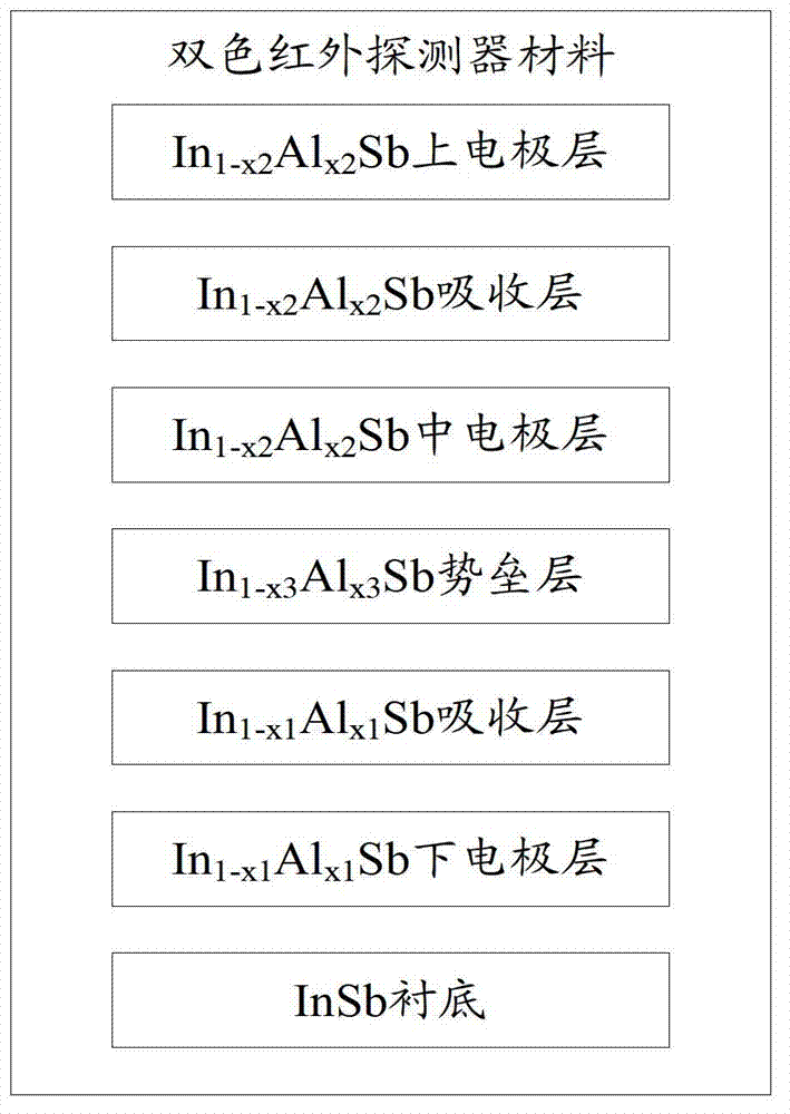
[0073] An embodiment of the present invention provides a two-color infrared detector material, such as figure 2 As shown, the two-color infrared detector material is a two-color infrared detector material obtained according to any of the above-mentioned methods, and the two-color infrared detector material comprises in turn: InSb substrate, In 1-x1 al x1 Sb lower electrode layer, In 1-x1 al x1 Sb absorption layer, In 1-x3 al x3 Sb barrier layer, In 1-x2 al x2 Sb middle electrode layer, In 1-x2 al x2 Sb absorber layer and In 1-x2 al x2 Sb upper electrode layer;

[0074] in,

[0075] The In 1-x1 al x1 The thickness of the growth of the Sb lower electrode layer is 0.5-3μm, and the n-type doping concentration is 2×10 17 -6×10 18 cm -3 cm -3 ;

[0076] The In1- x1 al xl The thickness of Sb absorbing layer growth is 0.5-6μm, without doping, and the concentration is controlled at 2×10 14 -5×10 16 cm -3 ;

[0077] The In 1-x3 al x3The thickness of Sb barrier...


PUM

PropertyMeasurementUnit
Thicknessaaaaaaaaaa
Thicknessaaaaaaaaaa
Thicknessaaaaaaaaaa

Abstract

The invention discloses a two-color infrared detector material and a preparation method thereof. The method comprises the steps of pre-treating an indium antimonide (InSb) crystal to obtain an epitaxial-level InSb substrate; and setting a parameter of an aluminium (Al) component in indium aluminium antimonide (InAlSb) according to a response wavelength range, and growing a lower electrode layer, an absorption layer, a barrier layer, a middle electrode layer, an absorption layer and an upper electrode layer of the InAlSb on the epitaxial-level InSb substrate sequentially, wherein the growth temperature is within a range of 400-450 DEG C, and the Sb/(In+Al) beam ratio is within a range of 1.2-10. By the aid of the two-color infrared detector material, two different wavelength ranges can be detected simultaneously, detection limits of environments on a two-color infrared detector are greatly reduced, and the detection effect is improved.

Description

technical field [0001] The invention relates to the field of materials, in particular to a two-color infrared detector material and a preparation method thereof. Background technique [0002] Infrared detectors have been widely used in early warning satellites, missile detection, lidar, communications, night vision, and infrared imaging due to their excellent performance. However, with the continuous development of existing infrared detectors, infrared stealth technology is also constantly Improvement, by making the target and the environmental background have similar emissivity in a specific waveband, resulting in a decrease in the contrast of the infrared target and making it difficult to identify, so the current two-color infrared detector material needs to be further improved. Contents of the invention [0003] In view of the above analysis, the present invention aims to provide a two-color infrared detector material and a preparation method thereof, so as to further i...

Claims


Application Information

Patent Timeline
IPC IPC(8): H01L31/18H01L31/0304
CPCY02P70/50
Inventor 刘铭巩锋程鹏王经纬邢伟荣
Owner 11TH RES INST OF CHINA ELECTRONICS TECH GROUP CORP
Why Eureka
Try Eureka