Unlock instant, AI-driven research and patent intelligence for your innovation.

Method for manufacturing oversize printed circuit board (PCB) back plate inner layer

A production method and super-sized technology, which is applied in the field of super-sized PCB backplane inner layer production, can solve problems such as short-circuit scrapping of the backplane inner layer, A/B deviation, etc., and achieve the effect of avoiding alignment deviation and accurate alignment

Inactive Publication Date: 2013-07-24
SHENZHEN SUNTAK MULTILAYER PCB
View PDF6 Cites 14 Cited by
  • Summary
  • Abstract
  • Description
  • Claims
  • Application Information

AI Technical Summary

Problems solved by technology

[0005] For this reason, the object of the present invention is to provide a method for making the inner layer of a super-large PCB backplane, which is mainly used to solve the problem of A / B deviation easily occurring when the current backplane with a size larger than 660mm*810mm is subjected to exposure processing, resulting in The problem of short-circuiting and scrapping the inner layer of the board

Method used


Image

  • Method for manufacturing oversize printed circuit board (PCB) back plate inner layer

Examples


Embodiment Construction

[0021] In order to illustrate the idea and purpose of the present invention, the present invention will be further described below in conjunction with the accompanying drawings and specific embodiments.

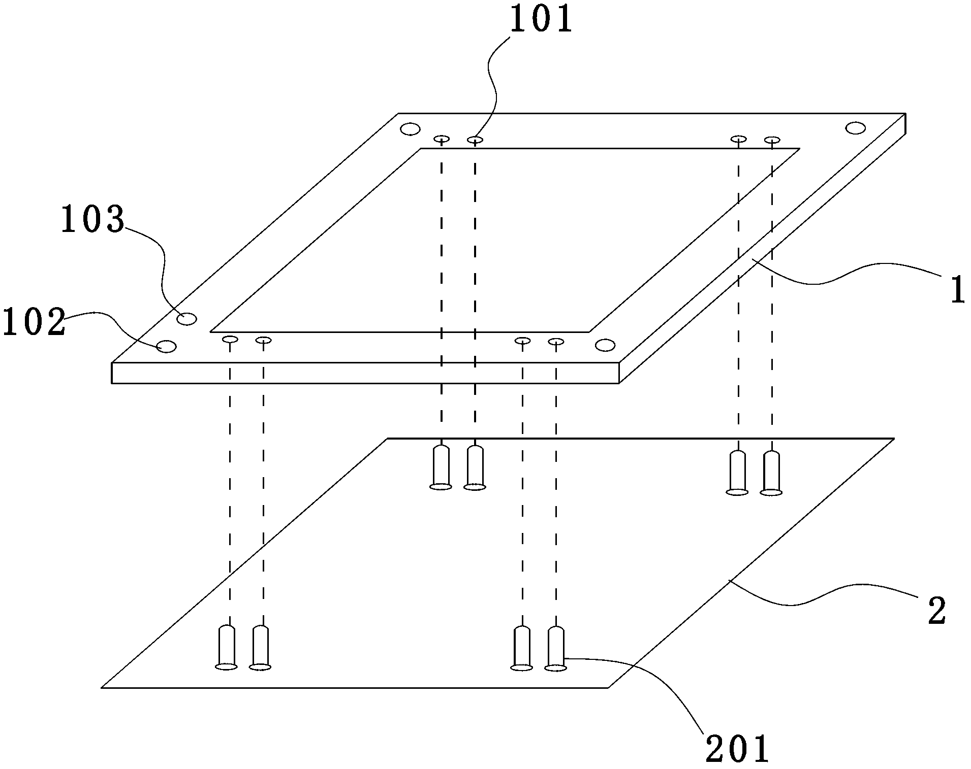
[0022] See figure 1 as shown, figure 1 It is a schematic diagram of the positioning state of the super-sized PCB backboard inner layer board and the film negative in the present invention. The present invention provides a method for manufacturing the inner layer of a super-sized PCB backplane, comprising steps:

[0023] S1. Cut the material to make the inner core board, and drill two PIN nail holes with a diameter of 2.1mm and one alignment inspection hole with a diameter of 3.175mm at the four corners of the inner core board;

[0024] First, cut the copper clad laminate, and make the inner core board 1 according to the normal method, and then design a special PIN drill strip for the board edge of the inner core board, because the size of the inner core board is larger , i...


PUM

PropertyMeasurementUnit
Diameteraaaaaaaaaa
Diameteraaaaaaaaaa
Diameteraaaaaaaaaa

Abstract

The invention discloses a method for manufacturing an oversize printed circuit board back plate inner layer. Firstly, a PIN tack hole is drilled on an edge plate position of an inner layer cross-band veneer; secondly, a PIN tack film photographic plate is manufactured; thirdly, a PIN tack column is arranged in a corresponding position of the film photographic plate and the PIN tack hole; fourthly, the PIN tack column of the film photographic plate is correspondingly sleeved in the PIN tack hole of the inner layer cross-band veneer; fifthly, single-face exposure is conducted on the inner layer cross-band veneer; and finally, all steps are conducted on the other face of the inner layer cross-band veneer, and single-face exposure is conducted on the other face of the inner layer cross-band veneer. Compared with traditional book clamping mode exposure, according to the method, the PIN tack hole in the inner layer cross-band veneer and the PIN tack column of a film photographic plate are mutually matched so as to realize accurate counterpoints, avoid the problem of counterpoint deviation between two faces of the same cross-band veneer, and solve the problem of scrap of the inner cross-band veneers. The scrap of the inner cross-band veneer is caused by a short circuit due to A / B deviation when exposure treatment is conducted on a back plate of size larger than 660mm*810mm.

Description

Technical field: [0001] The invention belongs to the technical field of printed circuit board manufacturing, and specifically relates to a method for manufacturing the inner layer of a super-large PCB backboard, mainly for backboards with a size larger than 660mm*810mm. Background technique: [0002] With the high integration of electronic components on the circuit board and the increase in the number of I / O, the advancement of electronic assembly technology, the high-frequency and high-speed digital development of signal transmission, and the upgrading and replacement needs of the rapid development of electronic equipment, PCB has gradually become The direction of bearing function sub-boards, signal transmission and power transmission is developing, while its signal processing function is gradually weakening. This type of PCB is the backplane. Backplane (Backplane or Back panel) refers to a type of printed circuit board with lines and many rows of jacks, mainly used to carr...

Claims


Application Information

Patent Timeline
IPC IPC(8): H05K3/46
Inventor 张军杰刘东李学明韩启龙
Owner SHENZHEN SUNTAK MULTILAYER PCB
Features
  • R&D
  • Intellectual Property
  • Life Sciences
  • Materials
  • Tech Scout
  • Unparalleled Data Quality
  • Higher Quality Content
  • 60% Fewer Hallucinations
Learn More