
Nano-devices formed with suspended graphene membrane

A graphene layer and device technology, applied in the fields of nanotechnology, nanotechnology, nanotechnology for materials and surface science, and can solve problems such as fragility

Inactive Publication Date: 2013-07-31
IBM CORP
View PDF3 Cites 11 Cited by
  • Summary
  • Abstract
  • Description
  • Claims
  • Application Information

AI Technical Summary

Problems solved by technology

To improve device sensitivity, electromechanical films must be made as thin as possible, which is problematic from a structural point of view because electromechanical films formed of metal films and silicon become very brittle when made thin

Method used


Image

  • Nano-devices formed with suspended graphene membrane
  • Nano-devices formed with suspended graphene membrane
  • Nano-devices formed with suspended graphene membrane

Examples


Embodiment Construction

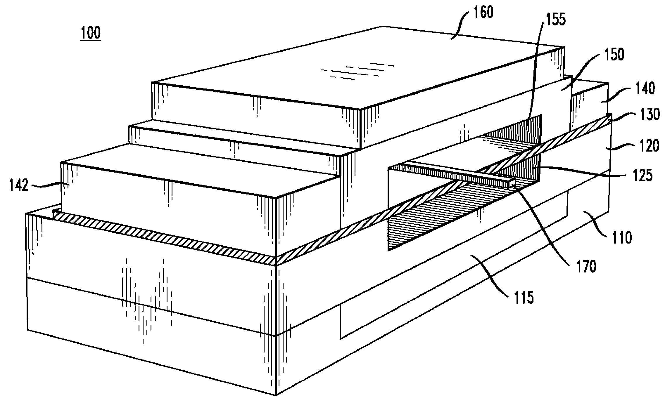
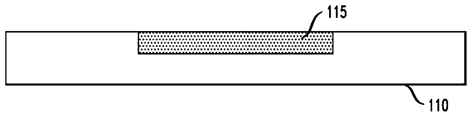
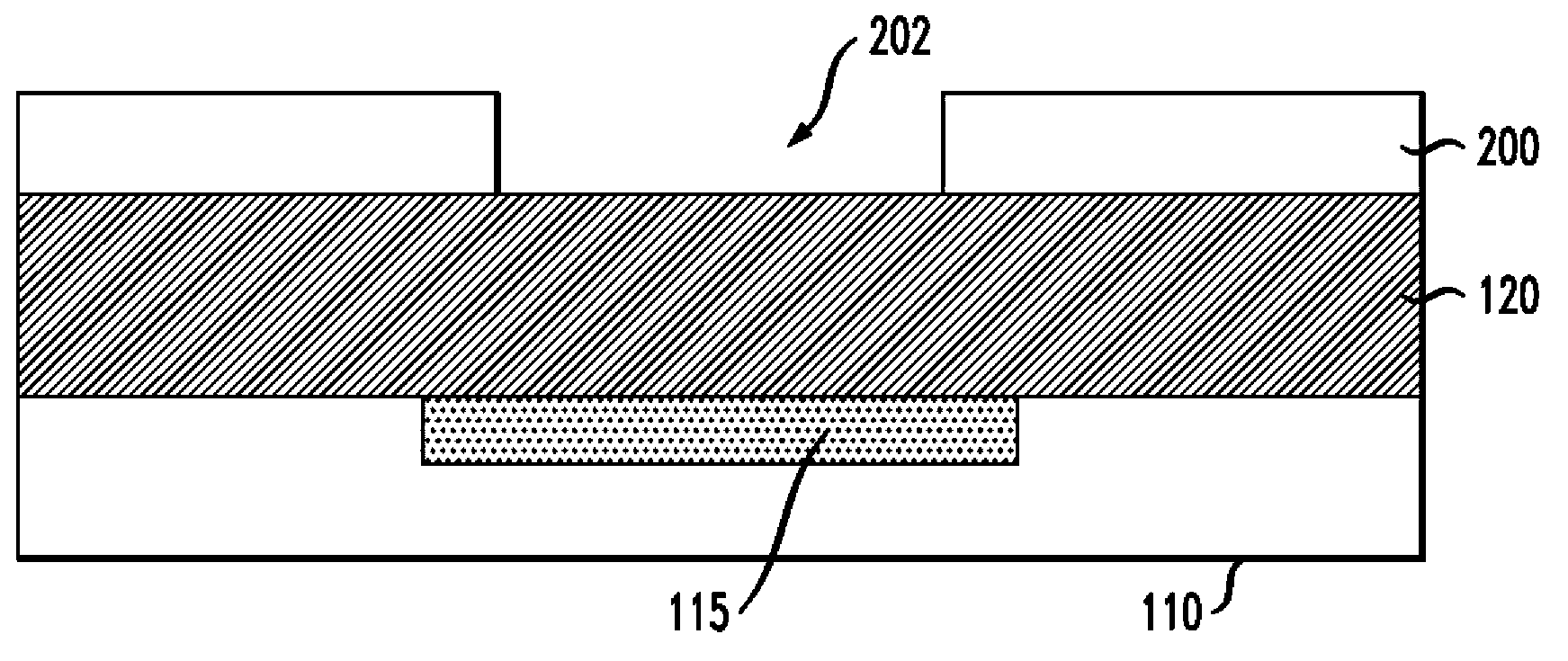
[0026] Preferred embodiments of the present invention will now be described in further detail with reference to semiconductor nanodevices, such as nanoprobe and nanoknife devices, constructed using electromechanical films made of graphene. For example, figure 1 is a 3D perspective view of a semiconductor nanodevice according to aspects of the invention. Generally speaking, the semiconductor nano-device 100 includes a bulk (bulk) substrate 110, a first gate electrode 115 (or bottom gate electrode) formed by doping a region of the substrate 100, a first cavity 125 (or lower cavity) First insulating layer 120, graphene film 130, second insulating layer 150 with second cavity 155 (or upper cavity), first sensing electrode 140, second sensing electrode 142 (wherein the second sensing electrode can be optional), second gate electrode 160 (or top gate electrode) and suspended between the first and second cavities 125 and 155 of the first and second insulating layers 120 and 150 moun...


PUM

PropertyMeasurementUnit
Widthaaaaaaaaaa

Abstract

Semiconductor nano-devices, such as nano-probe and nano-knife devices, which are constructed using graphene films that are suspended between open cavities of a semiconductor structure. The suspended graphene films serve as electro-mechanical membranes that can be made very thin, from one or few atoms in thickness, to greatly improve the sensitivity and reliability of semiconductor nano-probe and nano-knife devices.

Description

technical field [0001] The present invention relates generally to semiconductor nanodevices, and more particularly to semiconductor nanoprobes and nanometers constructed by mounting nano-probes or nanoknife on suspended graphene membranes. knife device. Background technique [0002] Nanoprobes and nanoknives are useful for applications such as medical diagnosis, surgery, and scientific experiments and as industrial sensors. Typically, the nanoprobe / knife is mounted on an electro-mechanical membrane. The electromechanical films of these devices are typically made of metal films or etched silicon layers. To improve device sensitivity, electromechanical films must be made as thin as possible, which is problematic from a structural point of view because electromechanical films formed of metal films and silicon become very brittle when made thin. Contents of the invention [0003] Aspects of the invention include semiconductor nanodevices, such as nanoprobe and nanoknife dev...

Claims


Application Information

Patent Timeline
IPC IPC(8): H01L29/78H01L29/06H01L21/336B82Y40/00
CPCB81B2203/0127H01L29/78606B81C1/00158B82Y40/00B82B3/00H01L29/06H01L29/78684H01L29/775B81B2201/038H01L29/78603H01L29/78648H01L29/78H01L29/4908B82Y30/00B82B1/00H01L29/1606H01L29/66045
Inventor 朱文娟
Owner IBM CORP
Learn More