Electro-optic conversion element and its application
An electro-optical conversion and component technology, applied in electrical components, circuits, semiconductor devices, etc., can solve problems such as unfavorable device integration, and achieve the effects of low cost, stable performance and simple processing
- Summary
- Abstract
- Description
- Claims
- Application Information
AI Technical Summary
Problems solved by technology
Method used
Image
Examples
Embodiment Construction
[0038] In order to make the purpose, technical solutions and advantages of the embodiments of the present invention more clear, specific embodiments will be described in detail below with reference to the accompanying drawings.
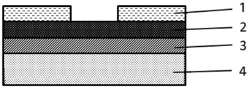
[0039] figure 1 A schematic structural view of an electro-optical conversion element according to an embodiment of the present invention is shown. Such as figure 1 As shown, the electro-optical conversion element of the embodiment of the present invention includes: a silicon oxide layer 3, two adjacent thin film strips 2 arranged on the silicon oxide layer 3, and two electrodes 1 respectively arranged on the two thin film strips 2 . In this embodiment, the silicon oxide layer 3 may consist of silicon oxide or mainly contain silicon oxide. There is a nano-gap between the two film strips 2 ( figure 1 Not shown in , see nanogap 503 shown in Figure 5(a)). Here, the material of the film strips has a melting point higher than that of silicon oxide, the...
PUM
 Abstract
Description
Claims
Application Information


