Non-volatile semiconductor storage device and method of manufacture thereof

A non-volatile, storage device technology, applied in the direction of semiconductor devices, electrical solid devices, electrical components, etc., can solve the problems of insufficient oxygen removal, insufficient molding process, and inability to perform stable resistance changes, etc., to achieve deviations in characteristics Small, high practical value effect

Active Publication Date: 2013-08-14
PANASONIC SEMICON SOLUTIONS CO LTD
View PDF4 Cites 3 Cited by
  • Summary
  • Abstract
  • Description
  • Claims
  • Application Information

AI Technical Summary

Problems solved by technology

However, in the variable resistance element having the above-mentioned oxidatively degraded layer, due to the resistance value of the parasitic resistance component included in the oxidatively degraded layer, a sufficient voltage may not be applied to the variable resistance element, and the molding process for starting oxidation and reduction reactions may not be sufficient. sufficient, stable resistance changes may not be possible
In addition, due to repeated rewriting operations, insufficient oxygen removal in the lower electrode may occur, and the oxygen concentration in the variable resistance layer may be increased to stop the phenomenon of resistance change, and the durability characteristics may be deteriorated.

Method used


Image

  • Non-volatile semiconductor storage device and method of manufacture thereof
  • Non-volatile semiconductor storage device and method of manufacture thereof
  • Non-volatile semiconductor storage device and method of manufacture thereof

Examples


Embodiment approach 1

[0056] First, the resistance variable nonvolatile semiconductor memory device in Embodiment 1 of the present invention will be described.

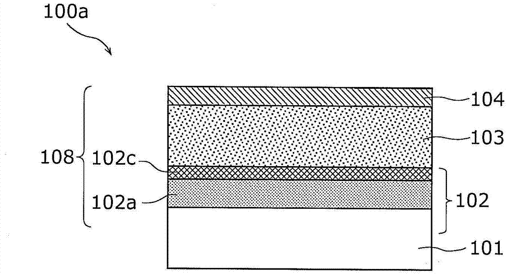
[0057] Figure 1A It is a cross-sectional view showing a configuration example of the variable resistance nonvolatile semiconductor memory device 100a according to the first embodiment of the present invention.

[0058] Such as Figure 1A As shown, the variable resistance nonvolatile semiconductor memory device 100a of the first embodiment includes: (1) a substrate 101; (2) a variable resistance element 108, which is composed of a lower electrode layer 102, an upper electrode layer 104, and The resistance variable layer 103 between these two electrodes is constituted.

[0059] The lower electrode layer 102 includes at least: (1) a first conductive layer 102a; (2) a second conductive layer 102c, which is formed on the first conductive layer 102a, and is a conductive layer in contact with the variable resistance layer 103 for making the lower part T...

Embodiment approach 2

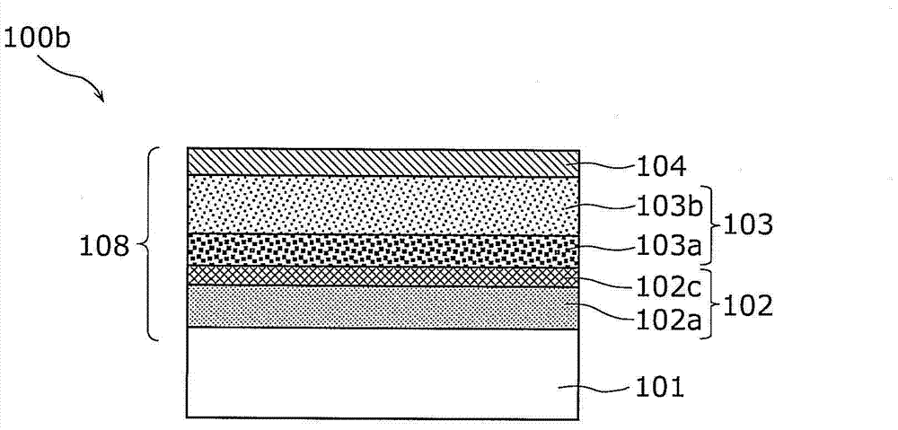
[0090] Next, a resistance variable nonvolatile semiconductor memory device in Embodiment 2 of the present invention will be described. In the first embodiment, the oxidative deterioration layer is not shown in the cross-sectional structure diagram of the nonvolatile semiconductor storage device, but in this embodiment, the oxidative deterioration layer is shown in the cross-sectional structure diagram of the nonvolatile semiconductor storage device. Layer and explain.

[0091] Figure 6A It is a cross-sectional view showing a configuration example of a variable resistance nonvolatile semiconductor memory device 200a according to Embodiment 2 of the present invention.

[0092] Such as Figure 6A As shown, the variable resistance nonvolatile semiconductor memory device 200a of the second embodiment includes: (1) a substrate 201; (2) a variable resistance element 208, which is composed of a lower electrode layer 202, an upper electrode layer 204, and The resistance variable layer 203...

Embodiment approach 3

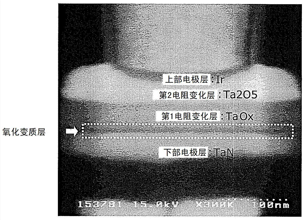
[0105] Next, a resistance variable nonvolatile semiconductor memory device in Embodiment 3 of the present invention will be described. The non-volatile semiconductor memory device of the present embodiment has a structure in which a non-ohmic element is laminated on the variable resistance element in the first embodiment.

[0106] Figure 7A It is a cross-sectional view showing a configuration example of a variable resistance nonvolatile semiconductor memory device 300a according to Embodiment 3 of the present invention.

[0107] Such as Figure 7A As shown, the variable resistance nonvolatile semiconductor memory device 300a of the third embodiment includes: (1) a substrate 301; (2) a variable resistance element 308, which is composed of a lower electrode layer 302, an upper electrode layer 304, and The resistance variable layer 303 between these two electrodes is composed; (3) The non-ohmic element 309 is composed of the first electrode layer 305, the semiconductor layer 306, and...


PUM


Abstract

Provided is a nonvolatile semiconductor memory device including a variable resistance element in which a parasitic resistance between the lower electrode and the variable resistance layer included in the variable resistance element is reduced. The nonvolatile semiconductor memory device includes: a substrate; and a variable resistance element formed on the substrate, wherein the variable resistance element includes a lower electrode layer formed on the substrate, a variable resistance layer formed on the lower electrode layer, and an upper electrode layer formed on the variable resistance layer, the lower electrode layer includes at least a first conductive layer and a second conductive layer which is formed on the first conductive layer and is in contact with the variable resistance layer, and the first conductive layer includes an oxidatively degraded layer which is formed on an upper surface of the first conductive layer due to oxidization of the first conductive layer.

Description

Technical field [0001] The present invention relates to a nonvolatile semiconductor storage device provided with a variable resistance element, and more particularly, to a configuration of a nonvolatile semiconductor storage device with excellent stability of operation and a method of manufacturing the same. Background technique [0002] In recent years, with the advancement of digital technology in electronic equipment, large-capacity and non-volatile semiconductor storage devices are being actively developed in order to store data such as music, images, and information. For example, nonvolatile semiconductor memory devices using ferroelectrics as capacitive elements have been used in many fields. In addition, unlike this type of nonvolatile semiconductor storage device using a ferroelectric capacitor, a resistance variable nonvolatile semiconductor storage device equipped with a variable resistance element (hereinafter also referred to as ReRAM) is easy to obtain the equivalent...

Claims


Application Information

Patent Timeline
Patent Type & Authority Applications(China)
IPC IPC(8): H01L27/105H01L45/00H01L49/00
CPCH01L45/16H01L49/00H01L45/1253H01L27/105H01L27/101H01L45/00H10B63/30H10B63/80H10N70/24H10N70/841H10N70/026H10N70/8833H10N70/011
Inventor 藤井觉伊藤理三河巧
Owner PANASONIC SEMICON SOLUTIONS CO LTD
Why Eureka
Try Eureka