Flexibly configured field-programmable gate array (FPGA) chip and configuration method thereof

A FAGA, chip technology, applied in sequence/logic controller program control, electrical program control, etc., can solve the problems of inflexible configuration method, uncontrollable configuration process, high configuration and working power consumption, etc.

Active Publication Date: 2013-08-21
CAPITAL MICROELECTRONICS
View PDF5 Cites 17 Cited by
  • Summary
  • Abstract
  • Description
  • Claims
  • Application Information

AI Technical Summary

Problems solved by technology

[0007] In view of this, the purpose of the present invention is to provide a flexible FPGA chip and configuration method thereof, to solve the problem that the FPGA chip configuration mode in the prior art is inflexible, the configuration process cannot be controlled, and the configuration and work power consumption are relatively large. question

Method used


Image

  • Flexibly configured field-programmable gate array (FPGA) chip and configuration method thereof
  • Flexibly configured field-programmable gate array (FPGA) chip and configuration method thereof
  • Flexibly configured field-programmable gate array (FPGA) chip and configuration method thereof

Examples


Embodiment Construction

[0017] The technical solutions of the present invention will be described in further detail below with reference to the accompanying drawings and embodiments.

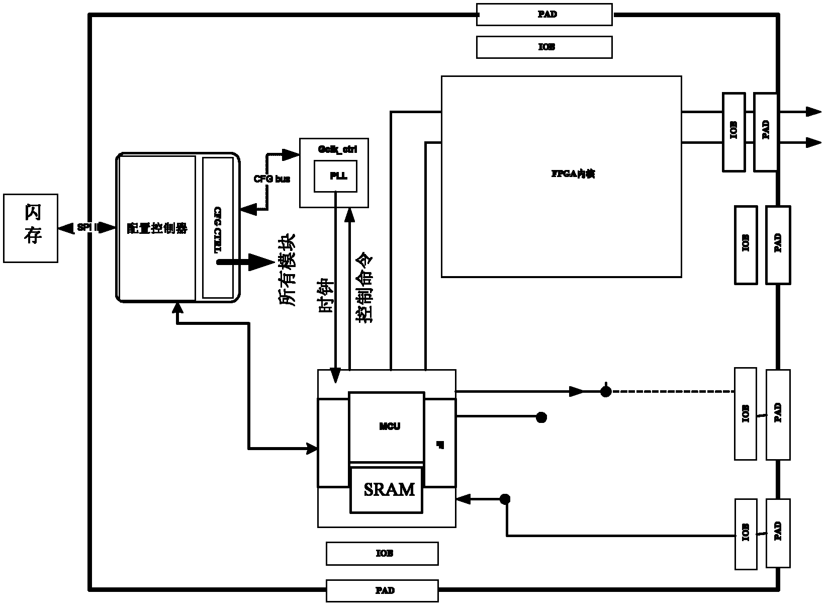
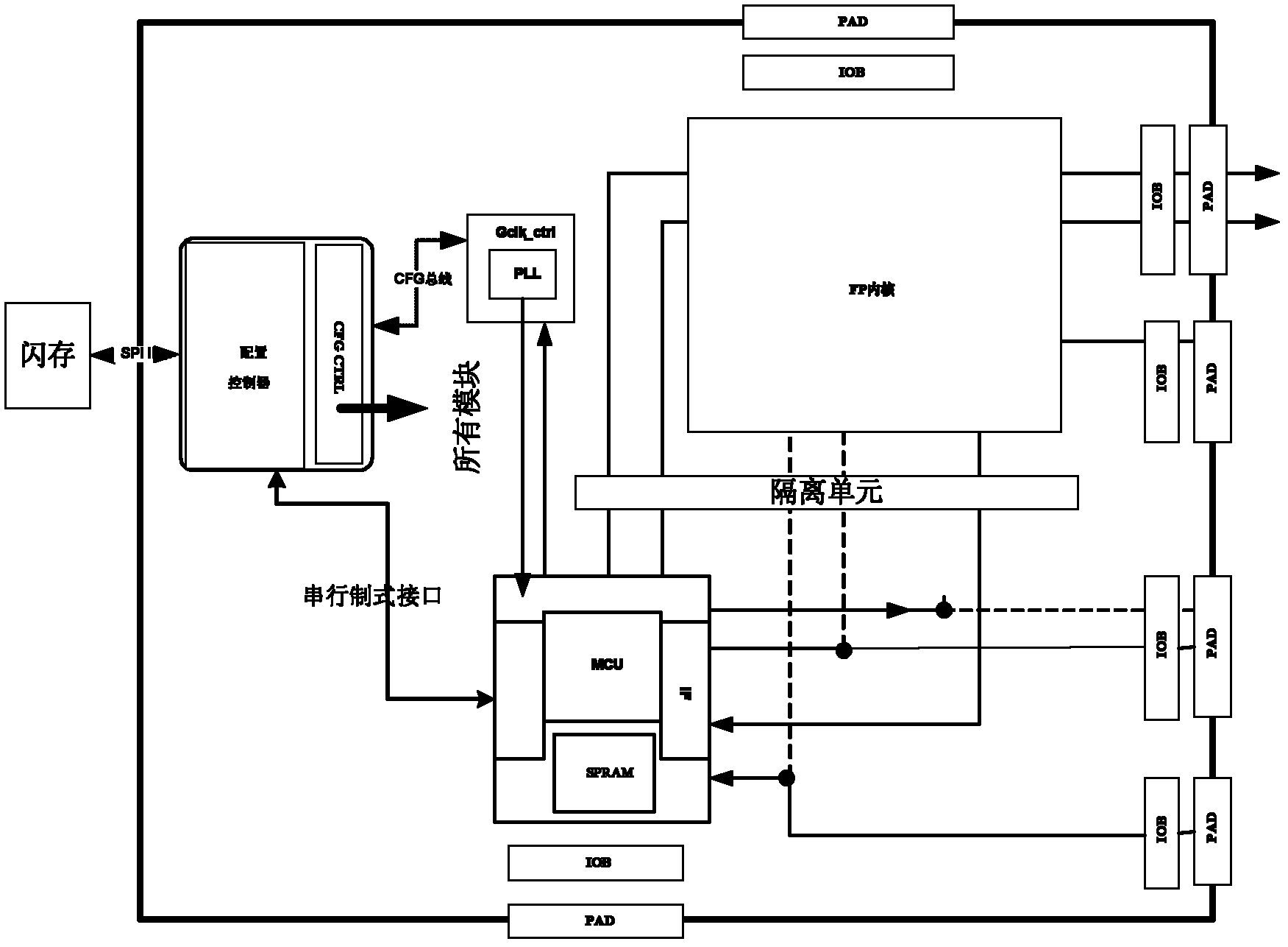
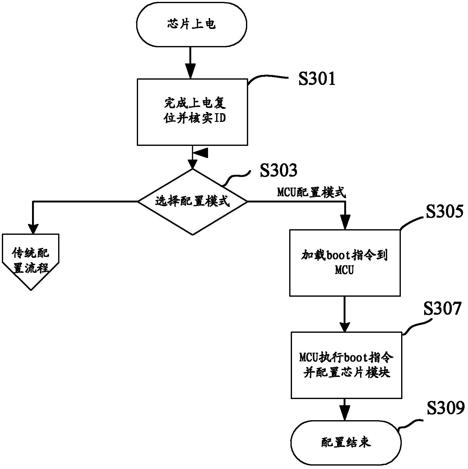
[0018] figure 1 It is a structural diagram of an FPGA chip according to an embodiment of the present invention. Such as figure 1 As shown, the FPGA chip includes several functional modules integrated in the same chip, the FPGA core module, the phase-locked loop module, the configuration controller config controller and the microprocessor MCU. Among them, the MCU is connected with a memory SRAM, which can read user programs or data. Several functional modules include, for example, an input / output unit IOB and the like. The FPGA core module is a specific array that completes the Field Programmable Logic Array. The configuration controller invokes the configuration program stored in the flash memory FLASH under the control of the MCU to configure one or more of the several functional modules of the FPGA chip, the FPGA...


PUM


Abstract

The invention relates to a flexibly configured field-programmable gate array (FPGA) chip and a configuration method of the FPGA chip. The chip comprises one or more of the following modules including an input / output module, an FPGA kernel module and a phase-locked loop module, wherein the one or more modules are integrated in the same chip. The chip further comprises a micro controller unit (MCU) and a configuration controller, the MCU is connected with a memorizer and used for controlling over the configuration of the FPGA chip, and under the control of the MCU, the configuration controller invokes configuration programs to carry out configuration on one or more of the FPGA kernel module, the input / output module and the phase-locked loop module of the FPGA chip. The method includes the steps: after power-on reset of a system, selecting a configuration mode, judging whether to select an MCU configuration mode or not, and if the MCU configuration mode is selected, loading a boot instruction to the MCU, executing the boot instruction by the MCU, and carrying out configuration on the whole chip. According to the technical scheme, flexible configuration of the FPGA chip can be achieved, and the effects that configuring efficiency is improved and power consumption is reduced are achieved.

Description

technical field [0001] The invention relates to the field of integrated circuits, in particular to a field programmable gate array FPGA chip with flexible configuration and a configuration method thereof. Background technique [0002] FPGA (Field-Programmable Gate Array), that is, Field Programmable Gate Array, is a product of further development on the basis of programmable devices such as PAL, GAL, and CPLD. It appears as a semi-custom circuit in the field of application-specific integrated circuits (ASIC), which not only solves the shortcomings of custom circuits, but also overcomes the shortcomings of the limited number of gate circuits of the original programmable device. [0003] FPGA adopts the concept of logic cell array LCA (Logic Cell Array), which includes three parts: configurable logic module CLB (Configurable Logic Block), input and output module IOB (Input Output Block) and internal wiring (Interconnect). Field Programmable Gate Arrays (FPGAs) are programmabl...

Claims


Application Information

Patent Timeline
Patent Type & Authority Applications(China)
IPC IPC(8): G05B19/05
Inventor 王军宁邹丽娜李大伟朱建彰王强
Owner CAPITAL MICROELECTRONICS
Why Eureka
Try Eureka