Memory cell of flash memory and forming method

A storage unit and flash memory technology, applied in electrical components, electric solid state devices, circuits, etc., can solve the problems of increasing the volume of flash memory devices, reducing the bit density of flash memory, and reducing bit cost, and achieves reduction in area, bit cost, etc. The effect of increasing the bit density

Active Publication Date: 2013-08-21
SEMICON MFG INT (SHANGHAI) CORP
View PDF4 Cites 8 Cited by
  • Summary
  • Abstract
  • Description
  • Claims
  • Application Information

AI Technical Summary

Problems solved by technology

[0010] However, there is a waste of space in the BiCS structure of the existing flash memory, resulting in a decrease in the bit density of the flash memory, an increase in the volume of the flash memory device, and a corresponding reduction in the bit cost. The manufacturing cost required for the storage space is a feature that reflects the cost of the storage device

Method used


Image

  • Memory cell of flash memory and forming method
  • Memory cell of flash memory and forming method
  • Memory cell of flash memory and forming method

Examples


Embodiment Construction

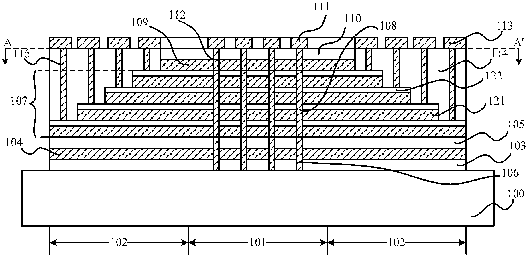
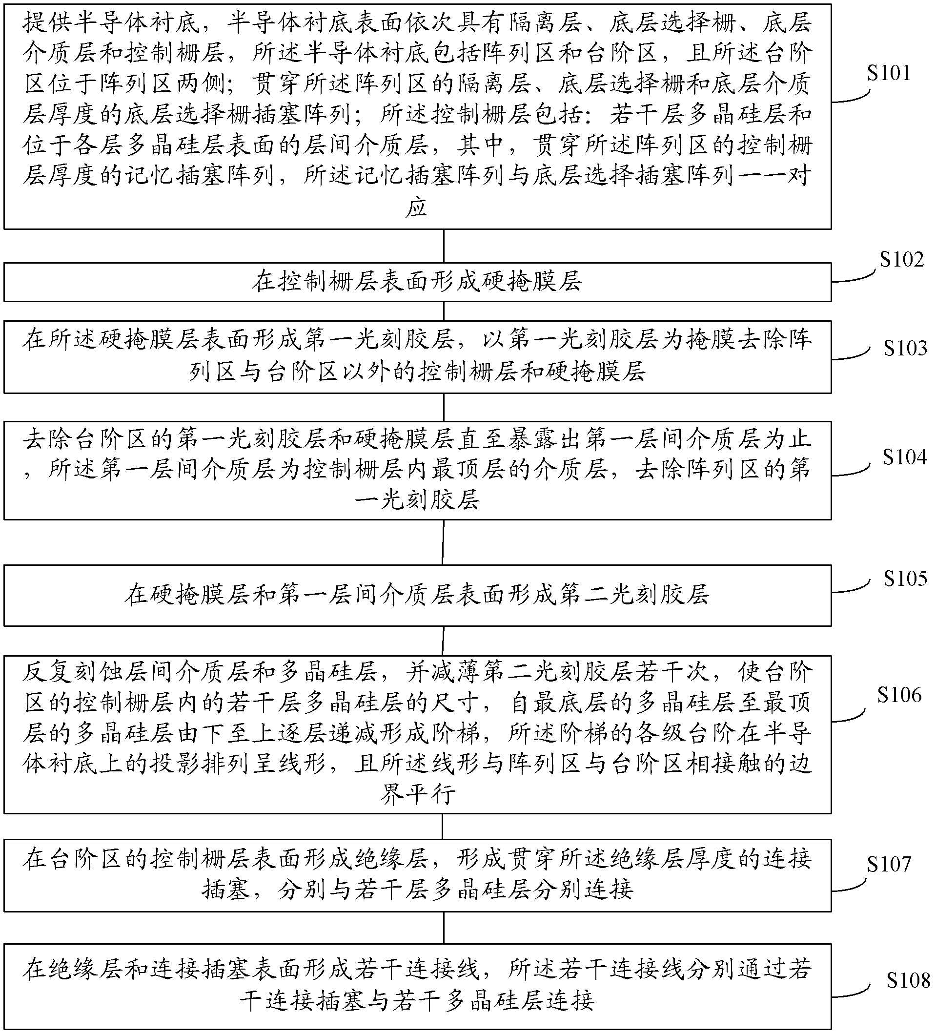
[0056] The inventors found that in the existing BiCS structure of flash memory, several layers of polysilicon layers in the control gate layer of flash memory are on the step region of the semiconductor substrate, from the position close to the array region to the outside of the array region from top to bottom layer by layer Incrementing forms a ladder shape, which causes a waste of space in the storage unit of the flash memory, thereby increasing the area of ​​the storage unit, thereby reducing the bit density of the flash memory and increasing the bit cost of the flash memory.

[0057] In order to reduce the area of ​​the storage unit of the flash memory, thereby increasing the bit density of the flash memory and reducing the bit cost of the flash memory, the inventor provides a storage unit of the flash memory, including:

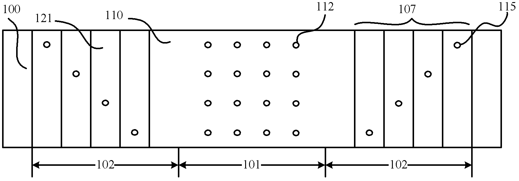
[0058] A semiconductor substrate, the semiconductor substrate includes an array area and a step area, the step area is on both sides of the array area; a...


PUM


Abstract

The invention discloses a memory cell of a flash memory and a forming method. The memory cell of the flash memory comprises a semiconductor substrate, an isolating layer, a base layer selecting grid, a base layer dielectric layer, control grid layers, a memory plugging array and a plurality of polycrystalline silicon layers. The semiconductor substrate comprises an array area and step areas and the step areas are arranged at two sides of the array area. The isolating layer, the base layer selecting grid and the base layer dielectric layer are sequentially arranged on the surface of the semiconductor substrate. The control grid layers are arranged on the surface of the base layer dielectric layer. The control grid layers further comprises a plurality of polycrystalline silicon layers and a plurality of interlayer dielectric layers arranged on the surfaces of the polycrystalline silicon layers. The memory plugging array penetrates through the control grid layers of the array area in a thickness direction. The polycrystalline silicon layers are arranged in the control grid layers of the step areas and form a ladder layer by layer from the lowermost layer to the topmost layer in a decreasing mode. Projections of steps of all levels of the ladder on the semiconductor substrate are arranged in the shape of a line, and the line is parallel to the boundaries of the array area and the step areas. According to the memory cell of the flash memory, bit density of the flash memory is improved, and cost is reduced.

Description

technical field [0001] The invention relates to a semiconductor device and a forming method thereof, in particular to a storage unit of a flash memory and a forming method thereof. Background technique [0002] In recent years, the development of flash memory (flash memory) is particularly rapid. The main feature of flash memory is that it can keep stored information for a long time without power on; and it has the advantages of high integration, fast access speed, easy erasing and rewriting, etc., so it has been widely used in many fields such as microcomputer and automatic control. a wide range of applications. [0003] In order to further increase the bit density of flash memory (bit density) and reduce the bit cost (bit cost), a low-cost three-dimensional stacked structure (Bit-Cost Scalable, referred to as BiCS) technology of flash memory has been further developed, please refer to figure 1 , is a schematic cross-sectional structure diagram of a memory cell of an exis...

Claims


Application Information

Patent Timeline
Patent Type & Authority Applications(China)
IPC IPC(8): H01L27/115H01L21/8247
Inventor 何其旸孟晓莹
Owner SEMICON MFG INT (SHANGHAI) CORP
Why Eureka
Try Eureka