Method for packaging organic electronic device

A technology of organic electronic devices and packaging methods, applied in the direction of electric solid devices, electrical components, semiconductor devices, etc., can solve the problems that rigid packaging cannot meet the packaging requirements of flexible devices, and achieve the goal of improving service life, reducing costs, and reducing thermal damage Effect

Inactive Publication Date: 2013-08-21
INST OF MICROELECTRONICS CHINESE ACAD OF SCI
View PDF5 Cites 22 Cited by
  • Summary
  • Abstract
  • Description
  • Claims
  • Application Information

AI Technical Summary

Problems solved by technology

[0005] The traditional rigid OLED and OPV device packaging is generally used in the glove box to cover the device with epoxy resin cured glass and other packaging covers, and combined with the use of dry film packaging, but the rigid packaging cannot meet the packaging requirements of flexible devices, and the flexible plastic substrate itself The water oxygen permeability is also higher than 10-5g / m 2 / day, which requires water and oxygen barrier isolation for flexible substrates

Method used


Image

  • Method for packaging organic electronic device

Examples


Embodiment Construction

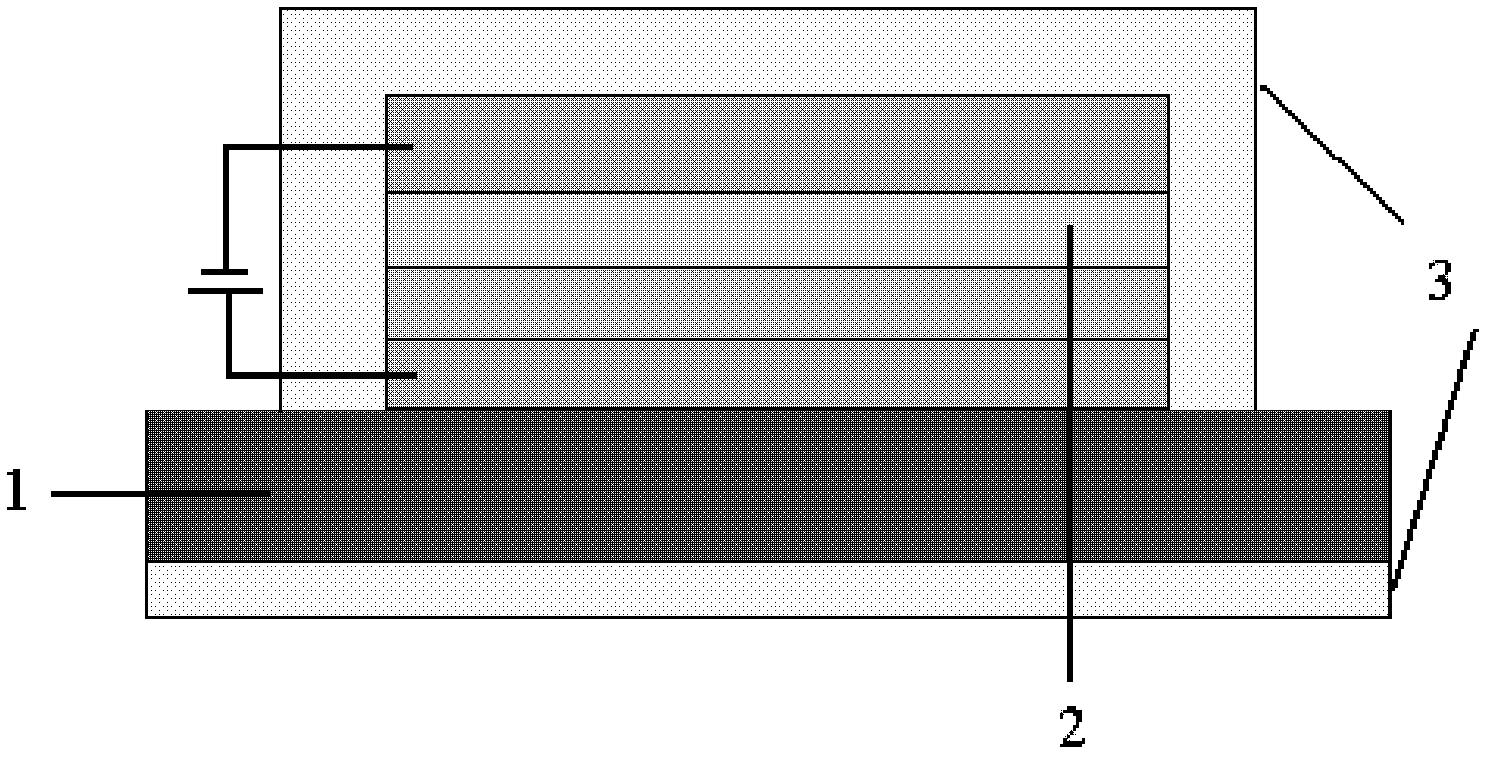
[0021] Such as figure 1 As shown, the packaging method of the organic electronic device provided by the present invention is divided into two steps, a pre-process and a post-process.

[0022] The previous process is to deposit a multi-layer composite thin film 3 on the back of the substrate 1 before making the organic electronic device 2 . A multi-layer composite thin film 3 is deposited by plasma enhanced chemical vapor deposition method (hereinafter referred to as PECVD method). The multilayer composite film 3 is composed of several layers of organic layers and inorganic layers alternately stacked. Organic layers are prepared from organic polymers including: parylene, polypropylene, polyacrylate or silicone crosslinked polymer SiO x C y h z . It is used to isolate water and oxygen; the inorganic layer is inorganic, which is used to increase flexibility, bendability and anti-breakage. The inorganic layer is prepared from inorganic substances, including: SiN x , SiO y ...


PUM


Abstract

The invention discloses a method for packaging an organic electronic device. The method for packaging the organic electronic device comprises the following steps that a plurality of layers of composite thin films are deposited on the back side of a lining material before the electronic device is prepared, the layers of composite thin films are deposited on the surface of the organic electronic device after the electronic device is prepared. By the adoption of a chip scale packaging method, a packaging process is integrated to a device manufacturing technological process, and therefore the original method of firstly manufacturing the device on a wafer and then the device is singly packaged after being cut is replaced. The method for packaging the organic electronic device has the advantages of improving efficiency and reducing cost. By the adoption of packaging through organic / inorganic layers of composite thin films in an innovative mode, water and oxygen can be isolated, therefore, the service life of the organic electronic device is greatly prolonged, flexible packaging can be achieved, and foldable and bending performance of the organic electronic device can be saved to the maximum. Eventually, according to the method for packaging the organic electronic device, low-temperature film formation below 120 DEG C is achieved, and heat damage to the device and plastic lining is reduced.

Description

technical field [0001] The invention relates to the field of electronic packaging, in particular to a method for packaging organic electronic devices. Background technique [0002] Organic optoelectronic devices have developed rapidly in the past two decades, especially organic light-emitting diodes (OLEDs), which have a series of advantages such as high luminous efficiency, low operating voltage, thinness and softness, and their related technologies and industries have attracted widespread attention. At present, the annual output value of OLED display exceeds one billion US dollars, and its products involve TV, MP3, mobile phone, car audio and so on. OSRAM, GE, Philips and other traditional global lighting giants have invested heavily in the field of OLED lighting and began to launch related products in 2009. According to the market analysis report of the professional organization NanoMarkets, the OLED display and lighting market will reach 10.9 billion US dollars in 2012. ...

Claims


Application Information

Patent Timeline
Patent Type & Authority Applications(China)
IPC IPC(8): H01L51/00
Inventor 吴茹菲刘键
Owner INST OF MICROELECTRONICS CHINESE ACAD OF SCI
Why Eureka
Try Eureka