Printed circuit board

A printed circuit board and electrical layer technology, which is applied to printed circuit components, electrical components, magnetic field/electric field shielding, etc., can solve problems affecting the stability of PCB boards, and achieve the effect of reducing the impact of interference

Inactive Publication Date: 2013-08-21
COMBA TELECOM SYST CHINA LTD
View PDF3 Cites 13 Cited by
  • Summary
  • Abstract
  • Description
  • Claims
  • Application Information

AI Technical Summary

Problems solved by technology

It will cause the surrounding environment to affect the radiation of the internal electrical layer power system of the PCB board and its high-speed sensitive printed lines, thereby affecting the stability of the entire PCB board, or the high speed of the inner electrical layer of the PCB board (above 5G) , The impact of high-frequency printed lines on the surrounding environment and equipment

Method used


Image

  • Printed circuit board
  • Printed circuit board
  • Printed circuit board

Examples


Embodiment Construction

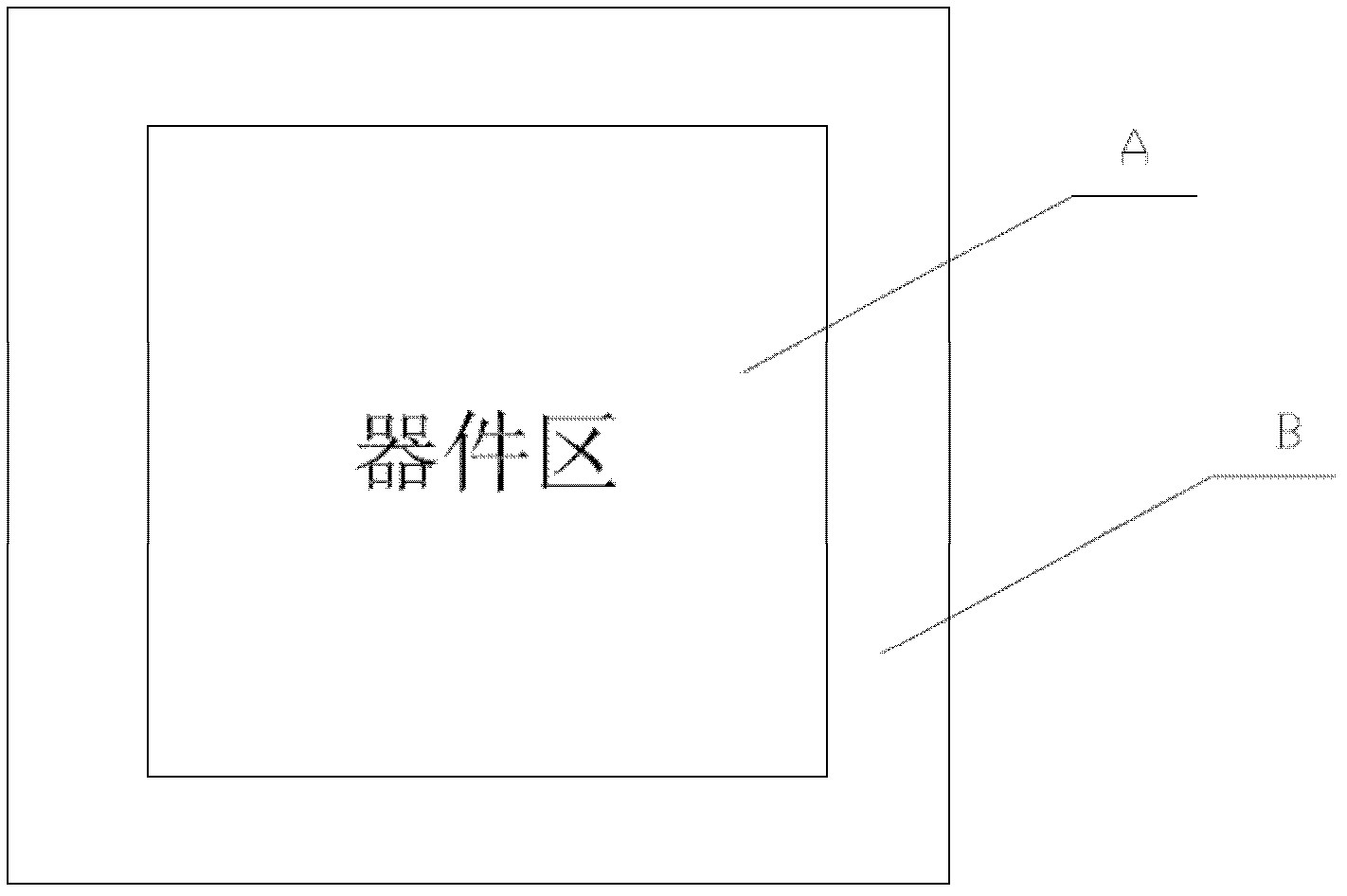
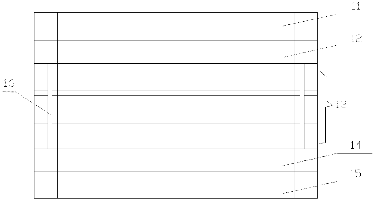
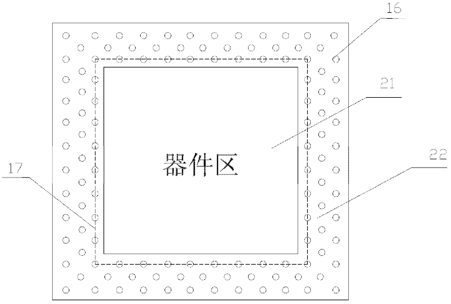
[0010] Please also see figure 2 and image 3 ,in, figure 2 It is a schematic cross-sectional structure diagram of the inner electrical layer PCB board 10 of the printed circuit board of the present invention, image 3 yes figure 2 The schematic diagram of the planar structure of the inner electric layer 13 is shown. The PCB board 10 includes a top device layer 11 , an upper ground layer 12 , an internal electrical layer 13 , a lower ground layer 14 and a bottom device layer 15 which are stacked in sequence. Wherein, a high-speed, high-frequency printed line (not shown) is arranged on the internal electrical layer 13 . The PCB board 10 is divided into a device area 21 and a shielding area 22 on a plane, wherein the device area 21 is arranged in the middle area of ​​the PCB board 10, and the shielding area 22 is arranged around the PCB board 10 and surrounds the device area twenty one. A plurality of conductive holes 16 are disposed in the shielding area 22 . The condu...


PUM


Abstract

The invention relates to a printed circuit board which comprises an upper ground layer, a lower ground layer and an inner electric layer arranged between the upper ground layer and the lower ground layer. The printed circuit board is characterized in that the upper ground layer and the lower ground layer are communicated through at least three conduction holes which are arranged by surrounding the inner electric layer, and a shielding net shielding the inner electric layer is formed by the upper ground layer, the lower ground layer and the conduction holes. The conduction holes surrounding the inner layer of the printed circuit board are provided, so that the upper ground layer and the lower ground layer of the printed circuit board and the conduction holes communicated with the upper ground layer and the lower ground layer form an almost-closed annular electromagnetic shielding cover so as to reduce disturbing influences on printed circuits and a power system of the inner electric layer of the printed circuit board by the outside, and therefore radiological hazards on external sensitive devices, equipment and human bodies by the inner electric layer of the circuit board are reduced.

Description

technical field [0001] The invention relates to a printed circuit board (PCB), in particular to a printed circuit board with the function of suppressing electromagnetic radiation. Background technique [0002] Printed circuit board (PCB), as the carrier of various electronic devices such as chips, is developing in the direction of high density, high speed, low power consumption, low cost and green environmental protection. Among them, it is mainly manifested in the following aspects: First, the printed line width of the PCB board is getting thinner and thinner, the thinnest has reached 1mil, and the number of layers is getting thinner and thinner, up to 40 layers. Secondly, as people's demand for information is increasing, which promotes the rapid development of electronic products, especially in the field of communication, the standard evolution from 3G to 4G. As a bridge for the interconnection between chipsets, the PCB board has been widely used in high-speed signaling, ...

Claims


Application Information

Patent Timeline
Patent Type & Authority Applications(China)
IPC IPC(8): H05K1/02H05K9/00
Inventor 张露露
Owner COMBA TELECOM SYST CHINA LTD
Why Eureka
Try Eureka