Liquid crystal panel and display device thereof

A liquid crystal panel and liquid crystal layer technology, applied in the direction of nonlinear optics, instruments, optics, etc., can solve the problems of long production time of liquid crystal panel and high complexity of liquid crystal panel process, and achieve improved ESD resistance, simple manufacturing process, damage reduction effect

Active Publication Date: 2013-09-04
XIAMEN TIANMA MICRO ELECTRONICS
View PDF13 Cites 12 Cited by
  • Summary
  • Abstract
  • Description
  • Claims
  • Application Information

AI Technical Summary

Problems solved by technology

[0008] Embodiments of the present invention provide a liquid crystal panel and a display device thereof, which are used to solve the problem of long production time and problems in the production of liquid crystal panels in order to prevent the internal electrode layer of the liquid crystal display panel from being affected by static electricity in the prior art. Problems with high process complexity

Method used


Image

  • Liquid crystal panel and display device thereof
  • Liquid crystal panel and display device thereof
  • Liquid crystal panel and display device thereof

Examples


Embodiment 1

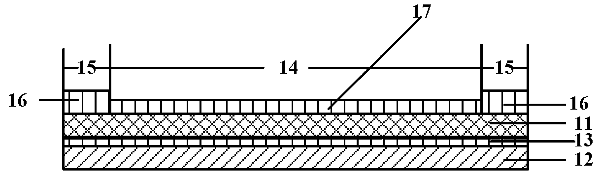
[0024] Such as figure 2 As shown, it is a schematic structure of a liquid crystal panel in the first embodiment. The liquid crystal panel includes: a first substrate 11 and a second substrate 12 oppositely arranged, and a liquid crystal layer 13 filled between the first substrate and the second substrate, the liquid crystal panel includes a display area 14 and a non-display area 15, The non-display area 15 is disposed around the display area 14, and a first shielding layer 16 is disposed on the non-display area 15 on the side away from the liquid crystal layer on the first substrate.

[0025] Preferably, the first substrate 11 is a color filter substrate, and the second substrate 12 is an array substrate.

[0026] Specifically, the first shielding layer 16 of the non-display area 15 may cover the entire non-display area of ​​the liquid crystal panel, or cover a part of the non-display area of ​​the liquid crystal panel according to actual needs, wherein the first shielding l...

Embodiment 2

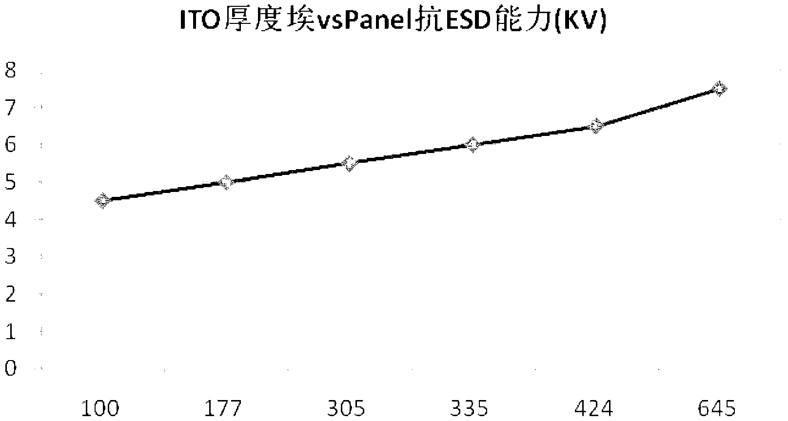
[0041]Assuming that the LCD panel adopts the IPS (In-Plane Switching, in-plane switching) mode, the first substrate is a color filter substrate, and the second substrate is an array substrate. Using the solution of Embodiment 1, set the first panel in the non-display area of ​​the color filter substrate. For the shielding layer, a second shielding layer is provided on the display area of ​​the color filter substrate, wherein the material of the first shielding layer and the second shielding layer is ITO.

[0042] Specifically, the thickness of the second shielding layer set in the display area is controlled at about 100 angstroms, while the thickness of the first shielding layer set in the non-display area can reach 600 angstroms, which not only ensures the display requirements of the display area, that is, the display area The second shielding layer can play the role of shielding the external electric field, so as to prevent the external electric field from interfering with th...

Embodiment 3

[0046] Such as Figure 7 As shown, it is a flowchart of a method for manufacturing a liquid crystal panel in Embodiment 3, and the method includes:

[0047] Step 101: providing a first glass substrate.

[0048] Step 102: Forming a first ITO layer on the first glass substrate by means of PVD coating.

[0049] Wherein, the first ITO layer in the display area of ​​the first glass substrate is the second shielding layer provided in the first embodiment.

[0050] Specifically, the thickness of the first ITO layer is 100 angstroms.

[0051] Step 103: After covering all the display areas on the first glass substrate with a mask, a second ITO layer is formed on the entire first glass substrate by PVD coating.

[0052] Wherein, the thickness of the second ITO layer is 500 angstroms.

[0053] It should be noted that the first ITO layer and the second ITO layer in the non-display area of ​​the first glass substrate are combined to form the first shielding layer provided in the first ...


PUM

PropertyMeasurementUnit
thicknessaaaaaaaaaa
thicknessaaaaaaaaaa
thicknessaaaaaaaaaa

Abstract

The invention discloses a liquid crystal panel and a display device of the liquid crystal panel. The liquid crystal panel mainly comprises a first substrate, a second substrate and a liquid crystal layer which is filled between the first substrate and the second substrate, wherein the first substrate and the second substrate are oppositely arranged. The liquid crystal panel comprises a display zone and a non-display zone, wherein the non-display zone surrounds the display zone. A first shielding layer is arranged on the non-display zone, far away from one side of the liquid crystal layer, on the first substrate. Compared with the prior art, the first shielding layer is arranged on the non-display zone, far away from the side of the liquid crystal layer, on the first substrate, manufacturing process is relatively simple, and when the liquid crystal panel is interfered by static, the first shielding layer can have the effect of resisting generated static, conductivity of the first shielding layer is utilized to release the generated static, the damage of the static to components inside the liquid crystal panel is reduced, and the capability of resisting ESD of the liquid crystal panel is improved.

Description

technical field [0001] The invention relates to the field of liquid crystal display, in particular to a liquid crystal display panel and a display device thereof. Background technique [0002] With the development of display technology, liquid crystal display devices are widely used in electronic products such as televisions, notebook computers, and mobile phones due to their advantages of light and thin appearance, low power consumption, and no radiation pollution. Among them, the liquid crystal display panel is a key component of the liquid crystal display device, and is mainly formed by combining two substrates and liquid crystal coated between the two substrates. The principle of liquid crystal display is to apply a voltage on the two substrates, and then under the action of the applied voltage, an electric field is formed between the two base stations. Under the action of the electric field, the liquid crystal molecules rotate and control the passage of the light beam t...

Claims


Application Information

Patent Timeline
Patent Type & Authority Applications(China)
IPC IPC(8): G02F1/1333
Inventor 陈晓和曾章和沈柏平林嘉民
Owner XIAMEN TIANMA MICRO ELECTRONICS
Why Eureka
Try Eureka