

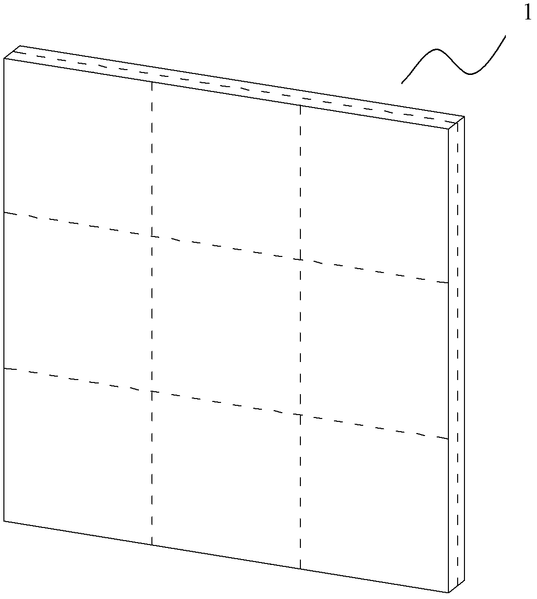
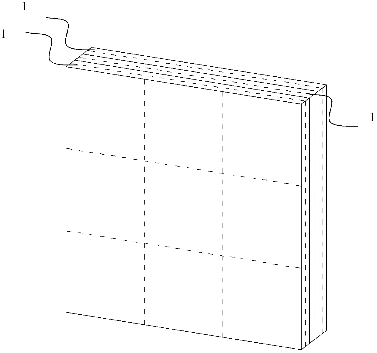
Low-loss metamaterial antenna housing
A metamaterial and radome technology, applied in the field of radome, can solve the problems of loss and poor wave transmission performance, and achieve the effects of enhanced wave transmission performance, increased anti-interference ability, and reduced material thickness and dielectric constant limitations
- Summary
- Abstract
- Description
- Claims
- Application Information
AI Technical Summary
Problems solved by technology
Method used
Image

Examples
Embodiment Construction
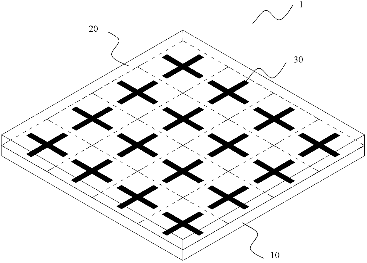
[0025] Metamaterials are artificial composite structural materials with extraordinary physical properties that natural materials do not have. Through the orderly arrangement of microstructures, the relative permittivity and magnetic permeability of each point in space can be changed. Metamaterials can realize within a certain range the refractive index, impedance, and wave-transmitting properties that ordinary materials cannot possess, so that they can effectively control the propagation characteristics of electromagnetic waves. The metamaterial radome based on the artificial microstructure can change the relative permittivity, refractive index and impedance of the material by adjusting the shape and size of the artificial microstructure, so as to achieve impedance matching with the air to maximize the incident electromagnetic wave. transmission. And the frequency can be selected by adjusting the size of the microstructure, and the corresponding wave-transmitting and filtering...
PUM
| Property | Measurement | Unit |
|---|---|---|
| Length | aaaaa | aaaaa |
| Width | aaaaa | aaaaa |
| Thickness | aaaaa | aaaaa |
Abstract
Description
Claims
Application Information