A printed circuit board and its processing method

A technology for printed circuit boards and circuits, which is applied to printed circuit components, and removes conductive materials by chemical/electrolytic methods. It can solve problems that affect signal accuracy, side erosion, and inability to protect, so as to ensure accuracy. , avoid side erosion phenomenon, high quality effect

Active Publication Date: 2016-09-21
SHENNAN CIRCUITS
View PDF3 Cites 0 Cited by
  • Summary
  • Abstract
  • Description
  • Claims
  • Application Information

AI Technical Summary

Problems solved by technology

[0003] However, during the subsequent etching process, the circuit 1 is only protected by a single-sided tin layer 2 on the upper surface, but cannot be protected on both sides, resulting in side etching, which in turn leads to a decrease in line width, etch factor and impedance. It is difficult to obtain higher quality, which seriously affects the accuracy of signal conduction and transmission, especially on high-density PCB boards, this defect is particularly prominent

Method used


Image

  • A printed circuit board and its processing method
  • A printed circuit board and its processing method
  • A printed circuit board and its processing method

Examples


Embodiment Construction

[0024] Embodiments of the present invention will be described in detail below in conjunction with the accompanying drawings.

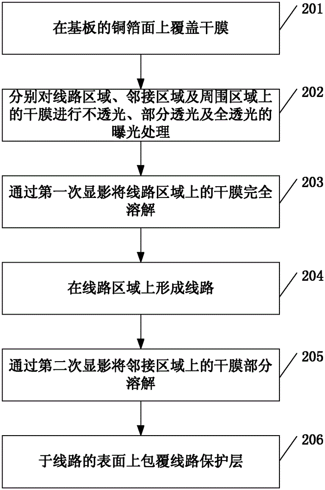
[0025] refer to figure 2 , the PCB processing method of the embodiment of the present invention mainly includes:

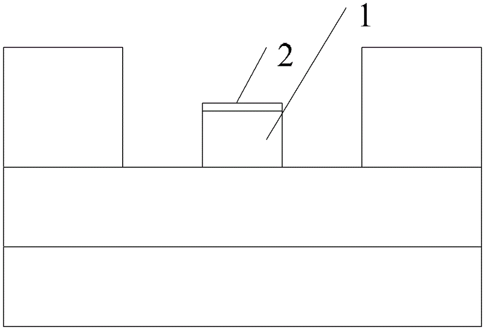
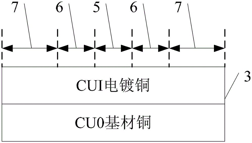
[0026] 201, covering the dry film 4 on the copper foil surface of the substrate 3, the copper foil surface includes the line area 5 and the non-line area for setting the line 1, and the non-line area includes the adjacent area 6 adjacent to the line area 5 and the surrounding area 7. Specifically, the circuit area 5, the adjacent area 6 and the surrounding area 7 on the copper foil surface can be as follows image 3 As shown, the structure formed after the substrate 3 covers the dry film 4 can be as follows Figure 4 shown;

[0027] 202. Perform opaque, partially transparent, and fully transparent exposure treatments on the dry film on the circuit area 5, the adjacent area 6, and the surrounding area 7 respectively. Specifically, the n...


PUM


Abstract

The invention discloses a printed circuit board and a processing method of the printed circuit board. The processing method comprises a first step of conducting lightproof, partial transmitting and full transmitting exposure treatment on dry film of a circuit area, dry film of an adjacent area and dry film of a peripheral area which are arranged on the surface of copper foil respectively, a second step of fully dissolving the dry film of the circuit area and forming a circuit on the circuit area by means of two-time developing in sequence, a third step of dissolving a part of dry film arranged on the adjacent area and remaining a dry film layer, a fourth step of wrapping the surface of the circuit with a circuit protective layer. Therefore, circuit protective layers cover the upper surface and the side surface of the circuit. The printed circuit board and the processing method of the printed circuit board have the advantages that when a follow-up etching technology is conducted, the circuit protective layer formed in all surfaces of the circuit can conduct multi-dimensional surface protection on the circuit, the phenomenon of lateral erosion is avoided, the higher quality on the aspects of the circuit width, etching factors and the precision of impendance of the printed circuit board circuit is guaranteed, and conduction and the precision of transmission of the circuit are ensured, especially for a high-precision printed circuit board plate, the advantages are more remarkable.

Description

technical field [0001] The invention relates to the field of printed circuit boards, in particular to a printed circuit board and a processing method thereof. Background technique [0002] In the printed circuit board (Printed Circuit Board, PCB) field, when using the additive process (graphic plating process) to make graphic circuits, usually a single-sided tin layer 2 is formed on the upper surface of the circuit 1 (such as figure 1 shown), so that the circuit is protected by a single-sided tin layer 2. [0003] However, during the subsequent etching process, the circuit 1 is only protected by a single-sided tin layer 2 on the upper surface, but cannot be protected on both sides, resulting in side etching, which in turn leads to a decrease in line width, etch factor and impedance. On the one hand, it is difficult to obtain higher quality, which seriously affects the accuracy of signal conduction and transmission, especially on high-density PCB boards, this defect is parti...

Claims


Application Information

Patent Timeline
Patent Type & Authority Patents(China)
IPC IPC(8): H05K3/06H05K1/02
Inventor 任文灿
Owner SHENNAN CIRCUITS
Why Eureka
Try Eureka